概要
説明
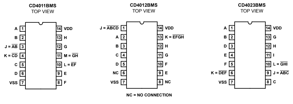
The CD4023BMS is a triple 3-input CMOS NAND gate that provides the system designer with direct implementation of the NAND function and supplements the existing family of CMOS gates. All inputs and outputs are buffered. The CD4023BMS is supplied in these 14-lead outline packages: Braze Seal DIP H4Q, Frit Seal DIP H1B and a Ceramic Flatpack H3W.
特長
- High-voltage types (20V rating)
- Propagation delay time = 60ns (typ.) at CL = 50pF, VDD = 10V
- Buffered inputs and outputs
- Standardized symmetrical output characteristics
- Maximum input current of 1µA at 18V over full package temperature range; 100nA at 18V and +25 °C
- 100% tested for maximum quiescent current at 20V
- 5V, 10V and 15V parametric ratings
- Noise margin (over full package temperature range):
- 1V at VDD = 5V
- 2V at VDD = 10V
- 2.5V at VDD = 15V
- Meets all requirements of JEDEC tentative standards No. 13B, "Standard Specifications for Description of "B" Series CMOS devices
製品比較
アプリケーション
ドキュメント
ピックアップ
ログイン後、ご登録が可能となります。
|
|
|
|
|---|---|---|
| 分類 | タイトル | 日時 |
| データシート | PDF 364 KB | |
| カタログ | PDF 467 KB | |
| 価格変更のお知らせ | PDF 360 KB | |
| その他資料 | ||
| 製品アドバイザリ | PDF 499 KB | |
| 製品変更通知 | PDF 230 KB | |
6件
|
||
設計・開発
モデル
ECADモデル
SamacSysの回路図シンボル、PCBフットプリント、および3D CADモデルは、製品オプションテーブルのCADモデルリンクをクリックすることで参照できます。シンボルまたはモデルが対応していない場合は、SamacSysに直接リクエスト可能です。

製品選択
適用されたフィルター