概要
説明
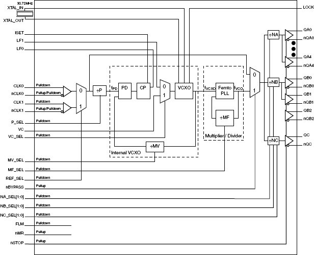
The 813076I is a member of the family of high performance clock solutions from IDT. The 813076I a PLL based synchronous clock solution that is optimized for wireless infrastructure equipment where frequency translation and jitter attenuation is needed.
The device contains two internal PLL stages that are cascaded in series. The first PLL stage attenuates the reference clock jitter by using an internal or external VCXO circuit. The internal VCXO requires the connection of an external inexpensive pullable crystal (XTAL) to the 813076I. This first PLL stage (VCXO PLL) uses external passive loop filter components which are used to optimize the PLL loop bandwidth and damping characteristics for the given application. The output of the first stage VCXO PLL is a stable and jitter-tolerant reference input for the second PLL stage of 30.72MHz. The second PLL stage provides frequency translation by multiplying the output of the first stage up to 614.4MHz. The low phase noise characteristics of the clock signal is maintained by the internal FemtoClock® PLL, which requires no external components or configuration. Two independently configurable frequency dividers translate the 491.52MHz or 614.4MHz internal VCO signal to the desired output frequencies. All frequency translation ratios are set by device configuration pins. Alternative to the clock frequency multiplication functionality, the 813076I can work as a VCXO. Enabling the VCXO mode allows the output frequency of 614.4MHz/N or 491.52MHz/N to be pulled by the input voltage of the VC pin.
特長
- Two operation modes: input frequency multiplier and VCXO
- Nine differential LVPECL outputs, organized in three independent output banks
- Two selectable differential input clocks can accept the following differential input levels: LVDS, LVPECL, LVHSTL, SSTL, HCSL
- Maximum output frequency: 614.4MHz
- FemtoClock VCO frequency: 491.52MHz or 614.4MHz (typical)
- Frequency generation optimized for wireless infrastructure equipment
- Attenuates the phase jitter of the input clock signal by using a low-cost pullable fundamental mode crystal (XTAL)
- Multiplies the input clock frequency by 1, 4, 5, 16 or 20
- LVCMOS/LVTTL levels for all input/output controls
- PLL fast-lock control
- VCXO PLL bandwidth can be optimized for jitter attenuation and reference frequency tracking using external loop filter components
- Absolute pull range: ±50ppm
- RMS phase jitter (12kHz - 20MHz): 0.97ps (typical)
- Full 3.3V supply
- -40°C to 85°C ambient operating temperature
- Available in lead-free (RoHS 6) package
- For other devices supporting wireless infrastructure clock frequencies, please refer to 813076I-02, 813076I-30, 813076I-31 and 814075
- For replacement device use 8T49N286-dddNLGI
製品比較
アプリケーション
設計・開発

製品選択
適用されたフィルター