Overview
Description
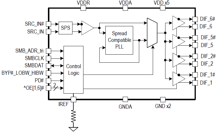
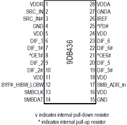
The 9DB436 is a zero delay/fanout buffer for PCI Express™ clocking. It supports PCIe Gen 1–3 in zero delay mode and PCIe Gen 1–4 in fanout mode. The 9DB436 also features a Safe Power Sequence (SPS) clock input. The 9DB436 is a pin-compatible upgrade to the 9DB433 and 9DB434.
Features
- Four 0.7V current-mode differential HCSL output pairs
- PCIe Gen 3 jitter < 0.6ps RMS in ZDB mode
- PCIe Gen 4 additive jitter < 0.1ps RMS in fanout mode
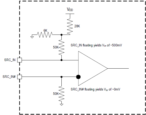
- SPS internal receiver bias network keeps the input clock parked when input is floating
- Supports both 85Ω and 100Ω output impedance with appropriate resistor selection
- OE# pins default to controlling outputs
- Supports zero delay buffer mode and fanout mode
- Selectable PLL bandwidth; minimizes jitter peaking in downstream PLLs
- Spread spectrum compatible
- Three selectable SMBus addresses
Comparison
Applications
Applications
- Riser cards
- Storage
- Networking
- JBOD
Design & Development
Models
ECAD Models
Schematic symbols, PCB footprints, and 3D CAD models from SamacSys can be found by clicking on products in the Product Options table. If a symbol or model isn't available, it can be requested directly from the website.

| TSSOP | 28 | I | Yes | Tube | ||
| TSSOP | 28 | I | Yes | Reel |

Tips for Using This Parametric Table:
- Hide Filters button in header: Collapse or expands filters
- Column sort buttons in header: Sort Column alphabetically / numerically descending or ascending
- Reset button in header: Reset all filters to the page default
- Full Screen button in header: Expand the table to full screen view (user must close out of full screen before they can interact with rest of page)
- Export button in header: Export the filtered results of the table to an Excel document
- Filter parts search bar in header: Type to filter table results by part number
- Hide column button in column headers: Select to hide columns in table
- AND / OR toggle switches in header: Toggles the logic of this particular filter to be “AND” or “OR” logic for filtering results
- Multiselect checkboxes at beginning of each row in table: Select these checkboxes to compare products against each other
- Document icon next to product name in row: View the featured document for this product
- Chip icon next to the right of the document icon in row: View the block diagram for this product
- Cart icon to the right of the chip icon: Indicates that samples are available for this product
Videos & Training
This is the first video in our PCIe series. In this video, we define PCIe architectures, focusing on common and separate clock architectures. Watch the rest of the video series below where Ron will cover the impact of different timing architectures.
Watch the Video Series Below
News & Blog Posts
| Blog Post | Apr 14, 2022 | ||
| Blog Post | May 22, 2018 | ||
| News | Apr 30, 2018 |


