Overview
Description
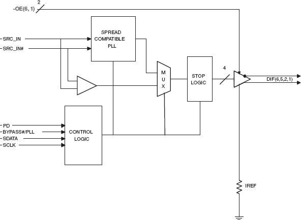
The 9DB403 is compatible with the Intel DB400v2 Differential Buffer Specification. This buffer provides 4 PCI Express® Gen2 clocks. The 9DB403 is driven by a differential output pair from a CK410B+, CK505 or CK509B main clock generator.
Features
- 4 - 0.7 V current-mode differential output pairs
- Supports zero delay buffer mode and fanout mode
- Bandwidth programming available
- 50-100 MHz operation in PLL mode
- 50-400 MHz operation in Bypass mode
- Spread spectrum modulation tolerant, 0 to -0.5% down spread and +/- 0.25% center spread.
- Supports undriven differential outputs in PD# and SRC_STOP# modes for power management.
- Outputs cycle-cycle jitter < 50 ps
- Outputs skew: 50 ps
- Phase jitter: PCIe Gen1 < 86 ps peak to peak
- Phase jitter: PCIe Gen2 < 3.0/3.1 ps rms
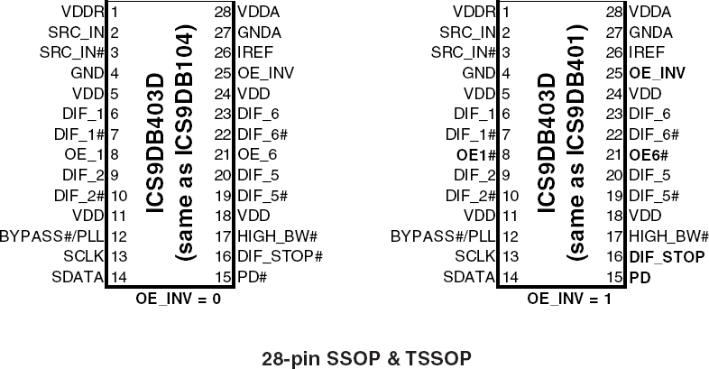
- 28-pin SSOP/TSSOP package
- Available in RoHS compliant packaging
- Supports Commercial (0 to +70°C) and Industrial (-40 to +85°C) temperature ranges
Comparison
Applications
Design & Development
Models
ECAD Models
Schematic symbols, PCB footprints, and 3D CAD models from SamacSys can be found by clicking on products in the Product Options table. If a symbol or model isn't available, it can be requested directly from the website.

Processing table
| SSOP | 28 | I | Yes | Tube | 3.035 | Get Samples, | |
| SSOP | 28 | I | Yes | Reel | |||
| SSOP | 28 | C | Yes | Tube | 2.833 | Get Samples, | |
| SSOP | 28 | C | Yes | Reel | 2.833 | ||
| TSSOP | 28 | I | Yes | Tube | 2.559 | Get Samples, | |
| TSSOP | 28 | I | Yes | Reel | 2.559 | ||
| TSSOP | 28 | C | Yes | Tube | 2.39 | Get Samples, | |
| TSSOP | 28 | C | Yes | Reel |

Tips for Using This Parametric Table:
- Hide Filters button in header: Collapse or expands filters
- Column sort buttons in header: Sort Column alphabetically / numerically descending or ascending
- Reset button in header: Reset all filters to the page default
- Full Screen button in header: Expand the table to full screen view (user must close out of full screen before they can interact with rest of page)
- Export button in header: Export the filtered results of the table to an Excel document
- Filter parts search bar in header: Type to filter table results by part number
- Hide column button in column headers: Select to hide columns in table
- AND / OR toggle switches in header: Toggles the logic of this particular filter to be “AND” or “OR” logic for filtering results
- Multiselect checkboxes at beginning of each row in table: Select these checkboxes to compare products against each other
- Document icon next to product name in row: View the featured document for this product
- Chip icon next to the right of the document icon in row: View the block diagram for this product
- Cart icon to the right of the chip icon: Indicates that samples are available for this product
Videos & Training
PCIe Clocking Architectures (Common and Separate)
This is the first video in our PCIe series. In this video, we define PCIe architectures, focusing on common and separate clock architectures. Watch the rest of the video series below where Ron will cover the impact of different timing architectures.
Watch the Video Series Below
Video List