Overview
Description
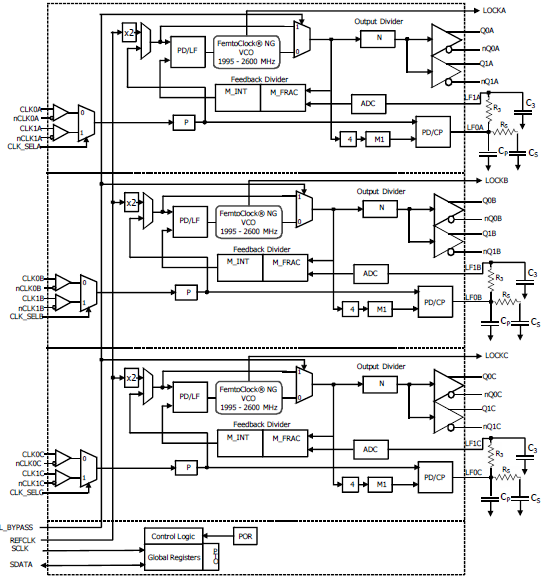
The 8T49N366I integrates low-phase noise frequency translation/synthesis and jitter attenuation. It includes alarm and monitoring functions suitable for networking and communications applications. The device has three fully independent PLLs. Each PLL can generate any output frequency in the 0.98MHz to 312.5MHz range and most output frequencies in the 312.5MHz to 1,300MHz range. A wide range of input reference clocks may be used as the source for the output frequency. Each 8T49N366I PLL has three operating modes to support a very broad spectrum of applications: Frequency Synthesizer, High-Bandwidth Frequency Translator, and Low-Bandwidth Frequency Translator.
To see other devices in this product family, visit the Universal Frequency Translators page.
Features
- Three fully independent PLLs
- Input frequency range: 8kHz to 710MHz
- Outputs are programmable as LVPECL or LVDS
- Programmable output frequency: 0.98MHz up to 1,300MHz
- Two differential inputs per PLL support the following input types: LVPECL, LVDS, LVHSTL, HCSL
- I²C serial interface for register programming
- RMS phase jitter: 465fs (typical), Low Bandwidth mode (FracN)
- RMS phase jitter: 333fs (typical), Synthesizer mode (Integer FB)
- Full 2.5V ±5% Supply mode
- -40 °C to 85 °C ambient operating temperature
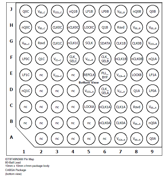
- 10mm x 10mm CABGA lead-free (RoHS 6) package
- Additional Family members include a dual PLL device, 8T49N244I, and quad PLL devices, 8T49N445I and 8T49N488I
Comparison
Applications
Design & Development
Models
ECAD Models
Schematic symbols, PCB footprints, and 3D CAD models from SamacSys can be found by clicking on products in the Product Options table. If a symbol or model isn't available, it can be requested directly from the website.

| CABGA | 80 | I | Yes | Tray | 3 | 67.04 | Get Samples, | |
| CABGA | 80 | I | Yes | Reel | 3 |

Tips for Using This Parametric Table:
- Hide Filters button in header: Collapse or expands filters
- Column sort buttons in header: Sort Column alphabetically / numerically descending or ascending
- Reset button in header: Reset all filters to the page default
- Full Screen button in header: Expand the table to full screen view (user must close out of full screen before they can interact with rest of page)
- Export button in header: Export the filtered results of the table to an Excel document
- Filter parts search bar in header: Type to filter table results by part number
- Hide column button in column headers: Select to hide columns in table
- AND / OR toggle switches in header: Toggles the logic of this particular filter to be “AND” or “OR” logic for filtering results
- Multiselect checkboxes at beginning of each row in table: Select these checkboxes to compare products against each other
- Document icon next to product name in row: View the featured document for this product
- Chip icon next to the right of the document icon in row: View the block diagram for this product
- Cart icon to the right of the chip icon: Indicates that samples are available for this product