Overview
Description
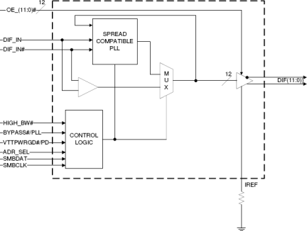
The 9DB1233 zero-delay buffer supports PCIe Gen3 requirements, while being backwards compatible to PCIe Gen2 and Gen1. The 9DB1233 is driven by a differential SRC output pair from an IDT 932S421 or 932SQ420 or equivalent main clock generator. It attenuates jitter on the input clock and has a selectable PLL bandwidth to maximize performance in systems with or without Spread-Spectrum clocking.
Features
- 12 - 0.7 V current mode differential HCSL output pairs
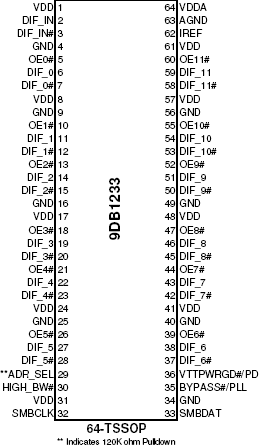
- 3 Selectable SMBus Addresses/Multiple devices can share the same SMBus Segment
- 12 OE# pins/Hardware control of each output
- PLL or bypass mode/PLL can dejitter incoming clock
- Selectable PLL bandwidth/minimizes jitter peaking in downstream PLL's
- Spread Spectrum Compatible/tracks spreading input clock for low EMI
- SMBus Interface/unused outputs can be disabled
- Supports undriven differential outputs in Power Down mode for power management
- Output cycle-cycle jitter < 50 ps
- Output-to-output skew < 50 ps
- PCIe Gen3 phase jitter < 1.0 ps RMS
- Pin compatible with DB1200 Yellow Cover Device
Comparison
Applications
Design & Development
Models
ECAD Models
Schematic symbols, PCB footprints, and 3D CAD models from SamacSys can be found by clicking on products in the Product Options table. If a symbol or model isn't available, it can be requested directly from the website.

Videos & Training
This is the first video in our PCIe series. In this video, we define PCIe architectures, focusing on common and separate clock architectures. Watch the rest of the video series below where Ron will cover the impact of different timing architectures.
Watch the Video Series Below
News & Blog Posts
| Blog Post | Apr 14, 2022 | ||
| Blog Post | May 22, 2018 | ||
| News | Apr 30, 2018 |


