Overview
Description
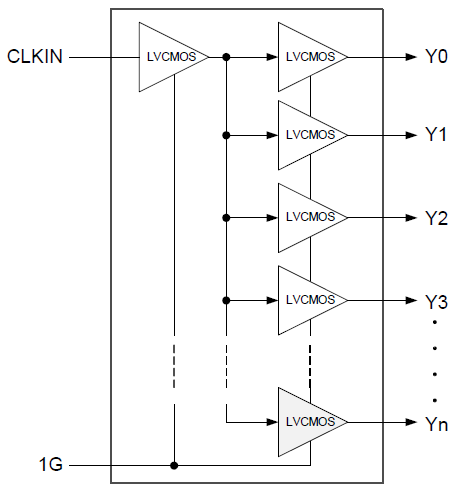
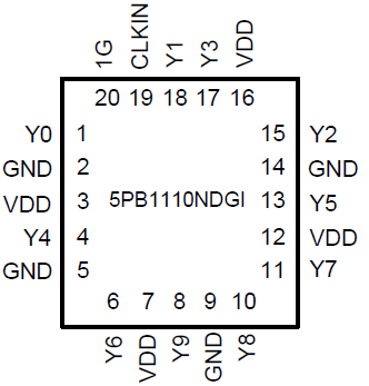
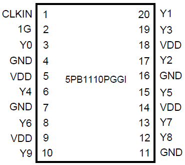
The 5PB1110 is a high-performance 1:10 LVCMOS clock buffer that offers a best-in-class additive phase jitter of 50fs RMS. This clock buffer also supports an Output Enable function. It is available in 20-pin QFN and TSSOP packages and can operate from a 1.8V to 3.3V supply.
Features
- High-performance 1:10 LVCMOS clock buffer
- Very low pin-to-pin skew: < 50ps
- Very low additive jitter: < 50fs
- Supply voltage: 1.8V to 3.3V
- fMAX = 200MHz
- Integrated serial termination for 50Ω channel
- Packaged in 20-pin TSSOP and small QFN packages
- Extended -40 °C to +105 °C temperature range
- AEC-Q100 qualified, Automotive Grade 2 (-40 °C to +105 °C)
Comparison
Applications
Applications
- Industrial applications
- Automotive
- Radar, LiDAR, and other applications
Design & Development
Models
ECAD Models
Schematic symbols, PCB footprints, and 3D CAD models from SamacSys can be found by clicking on products in the Product Options table. If a symbol or model isn't available, it can be requested directly from the website.

Processing table
Pkg. Type |
Lead Count (#) |
Temp. Range |
Description |
Carrier Type |
Moisture Sensitivity Level (MSL) |
Price (USD) | 1ku |
Buy / Sample |
|
|---|---|---|---|---|---|---|---|---|
| Part Number | ||||||||
| VFQFPN | 20 | -40 to 85°C | Tray | 1 | 2.828 | Get Samples, | ||
| VFQFPN | 20 | -40 to 85°C | Reel | 1 | 2.828 | |||
| TSSOP | 20 | -40 to 85°C | Tube | 1 | 3.353 | Get Samples, | ||
| TSSOP | 20 | -40 to 85°C | Reel | 1 | 2.5 | |||
| VFQFPN | 20 | -40 to 105°C | Tray | 1 | 3.353 | Get Samples, | ||
| VFQFPN | 20 | -40 to 105°C | Reel | 1 | ||||
| TSSOP | 20 | -40 to 105°C | Tube | 1 | 2.5 | Get Samples, | ||
| TSSOP | 20 | -40 to 105°C | Reel | 1 | ||||
| VFQFPN | 20 | -40 to 105°C | Automotive | Tray | 1 | 4.074 | Get Samples, | |
| VFQFPN | 20 | -40 to 105°C | Automotive | Reel | 1 |

Tips for Using This Parametric Table:
- Hide Filters button in header: Collapse or expands filters
- Column sort buttons in header: Sort Column alphabetically / numerically descending or ascending
- Reset button in header: Reset all filters to the page default
- Full Screen button in header: Expand the table to full screen view (user must close out of full screen before they can interact with rest of page)
- Export button in header: Export the filtered results of the table to an Excel document
- Filter parts search bar in header: Type to filter table results by part number
- Hide column button in column headers: Select to hide columns in table
- AND / OR toggle switches in header: Toggles the logic of this particular filter to be “AND” or “OR” logic for filtering results
- Multiselect checkboxes at beginning of each row in table: Select these checkboxes to compare products against each other
- Document icon next to product name in row: View the featured document for this product
- Chip icon next to the right of the document icon in row: View the block diagram for this product
- Cart icon to the right of the chip icon: Indicates that samples are available for this product
Videos & Training
5PB11xx Ultra Low Jitter LVCMOS Buffers
This video provides an overview of the LVCMOS High Performance Clock Buffer Family, highlighting their key features and capabilities.

Video List
News & Blog Posts
| Blog Post | Feb 7, 2019 | ||
| Blog Post | Dec 15, 2018 | ||
| News | Mar 24, 2015 |


