Overview
Description
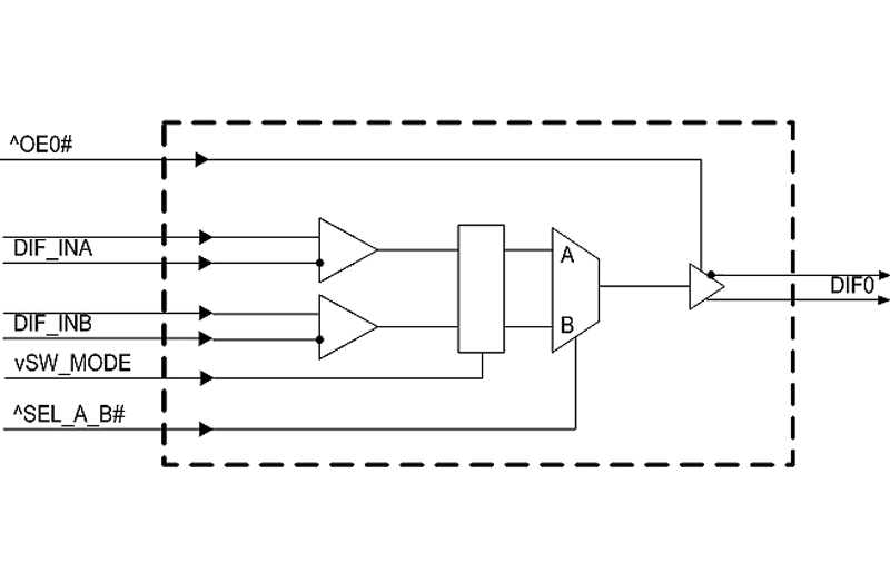
The 9DMV0131 is a member of Renesas' SOC-Friendly 1.8 V Very-Low-Power (VLP) PCIe Gen1–5 family. The output has an OE# pin for optimal system control and power management. The part provides asynchronous or glitch-free switching modes.
Features
-
LP-HCSL output; saves 2 resistors compared to standard HCSL output
-
1.8 V operation; 12 mW typical power consumption
-
Selectable asynchronous or glitch-free switching; allows the mux to be selected at power up even if both inputs are not running, then transition to glitch-free switching mode
-
Spread spectrum compatible; supports EMI reduction
-
OE# pin; supports DIF power management
-
HCSL differential inputs; can be driven by common clock sources
-
1 MHz to 200 MHz operating frequency
-
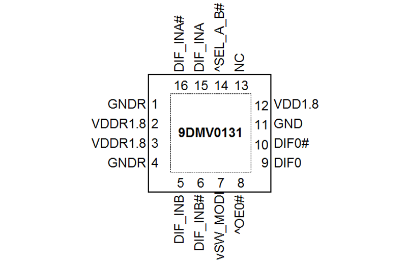
Space saving 3x3 mm 16-pin VFQFPN; minimal board space
Comparison
Applications
Design & Development
Models
ECAD Models
Schematic symbols, PCB footprints, and 3D CAD models from SamacSys can be found by clicking on products in the Product Options table. If a symbol or model isn't available, it can be requested directly from the website.

Processing table
| VFQFPN | 16 | I | Yes | Tray | 2.414 | Get Samples, | |
| VFQFPN | 16 | I | Yes | Reel |

Tips for Using This Parametric Table:
- Hide Filters button in header: Collapse or expands filters
- Column sort buttons in header: Sort Column alphabetically / numerically descending or ascending
- Reset button in header: Reset all filters to the page default
- Full Screen button in header: Expand the table to full screen view (user must close out of full screen before they can interact with rest of page)
- Export button in header: Export the filtered results of the table to an Excel document
- Filter parts search bar in header: Type to filter table results by part number
- Hide column button in column headers: Select to hide columns in table
- AND / OR toggle switches in header: Toggles the logic of this particular filter to be “AND” or “OR” logic for filtering results
- Multiselect checkboxes at beginning of each row in table: Select these checkboxes to compare products against each other
- Document icon next to product name in row: View the featured document for this product
- Chip icon next to the right of the document icon in row: View the block diagram for this product
- Cart icon to the right of the chip icon: Indicates that samples are available for this product
Videos & Training
PCIe Clocking Architectures (Common and Separate)
This is the first video in our PCIe series. In this video, we define PCIe architectures, focusing on common and separate clock architectures. Watch the rest of the video series below where Ron will cover the impact of different timing architectures.
Watch the Video Series Below
Video List