Overview
Description
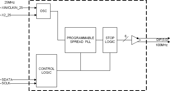
The 9FGL699 is a 6-output low-power clock sythesizer for PCIe Gen2. It runs from a 25 MHz XTAL, provides spread spectrum capability, and has an SMBus for software control of the device.
Features
- 6 - 100 MHz Differential low power push pull (HCSL compatible) output pairs
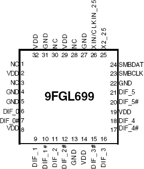
- 32-pin QFN; space-savings
- Push Pull outputs
- Low power consumption, reduced component count
- PCIe Gen2
- Spread spectrum capability; reduced EMI when needed
- D2/D3 SMBus Write/Read SMBus address
- Cycle-to-cycle jitter <125 ps
- Output-to-output skew < 100 ps
- Current consumption < 40 mA
- PCIe Gen2 phase jitter < 3.0 ps RMS
Comparison
Applications
Design & Development
Models
ECAD Models
Schematic symbols, PCB footprints, and 3D CAD models from SamacSys can be found by clicking on products in the Product Options table. If a symbol or model isn't available, it can be requested directly from the website.

Processing table
| VFQFPN | 32 | C | Yes | Tray | ||
| VFQFPN | 32 | C | Yes | Reel |

Tips for Using This Parametric Table:
- Hide Filters button in header: Collapse or expands filters
- Column sort buttons in header: Sort Column alphabetically / numerically descending or ascending
- Reset button in header: Reset all filters to the page default
- Full Screen button in header: Expand the table to full screen view (user must close out of full screen before they can interact with rest of page)
- Export button in header: Export the filtered results of the table to an Excel document
- Filter parts search bar in header: Type to filter table results by part number
- Hide column button in column headers: Select to hide columns in table
- AND / OR toggle switches in header: Toggles the logic of this particular filter to be “AND” or “OR” logic for filtering results
- Multiselect checkboxes at beginning of each row in table: Select these checkboxes to compare products against each other
- Document icon next to product name in row: View the featured document for this product
- Chip icon next to the right of the document icon in row: View the block diagram for this product
- Cart icon to the right of the chip icon: Indicates that samples are available for this product
Videos & Training
PCIe Clocking Architectures (Common and Separate)
This is the first video in our PCIe series. In this video, we define PCIe architectures, focusing on common and separate clock architectures. Watch the rest of the video series below where Ron will cover the impact of different timing architectures.
Watch the Video Series Below
Video List