Overview
Description
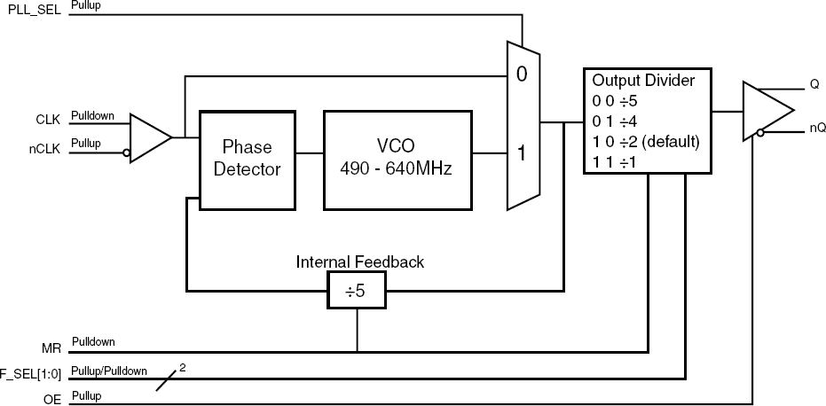
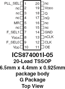
The 874001I-05 is a high performance Jitter Attenuator designed for use in PCI Express®™ systems. In some PCI Express® systems, such as those found in desktop PCs, the PCI Express® clocks are generated from a low bandwidth, high phase noise PLL frequency synthesizer. In these systems, a jitter attenuator may be required to attenuate high frequency random and deterministic jitter components from the PLL synthesizer and from the system board. The 874001I-05 has a bandwidth of 6MHz with <1dB peaking, easily meeting PCI Express® Gen2 PLL requirements. The 874001I-05 uses IDT's 3RD Generation FemtoClock® PLL technology to achieve the lowest possible phase noise. The device is packaged in a small 20-pin TSSOP package, making it ideal for use in space constrained applications such as PCI Express® add-in cards.
Features
- One differential LVDS output pair
- One differential clock input
- CLK, nCLK supports the following input levels: LVPECL, LVDS, LVHSTL, SSTL, HCSL
- Input frequency range: 98MHz to 128MHz
- Output frequency range: 98MHz to 640MHz
- VCO range: 490MHz - 640MHz
- Cycle-to-cycle jitter: 50ps (maximum)
- Full 3.3V operating supply
- PCI Express® (2.5Gb/s) and Gen 2 (5 Gb/s) jitter compliant
- -40°C to 85°C ambient operating temperature
- Available in lead-free (RoHS 6) package
Comparison
Applications
Design & Development
Models
ECAD Models
Schematic symbols, PCB footprints, and 3D CAD models from SamacSys can be found by clicking on products in the Product Options table. If a symbol or model isn't available, it can be requested directly from the website.

| TSSOP | 20 | I | Yes | Tube | ||
| TSSOP | 20 | I | Yes | Reel |

Tips for Using This Parametric Table:
- Hide Filters button in header: Collapse or expands filters
- Column sort buttons in header: Sort Column alphabetically / numerically descending or ascending
- Reset button in header: Reset all filters to the page default
- Full Screen button in header: Expand the table to full screen view (user must close out of full screen before they can interact with rest of page)
- Export button in header: Export the filtered results of the table to an Excel document
- Filter parts search bar in header: Type to filter table results by part number
- Hide column button in column headers: Select to hide columns in table
- AND / OR toggle switches in header: Toggles the logic of this particular filter to be “AND” or “OR” logic for filtering results
- Multiselect checkboxes at beginning of each row in table: Select these checkboxes to compare products against each other
- Document icon next to product name in row: View the featured document for this product
- Chip icon next to the right of the document icon in row: View the block diagram for this product
- Cart icon to the right of the chip icon: Indicates that samples are available for this product
Videos & Training
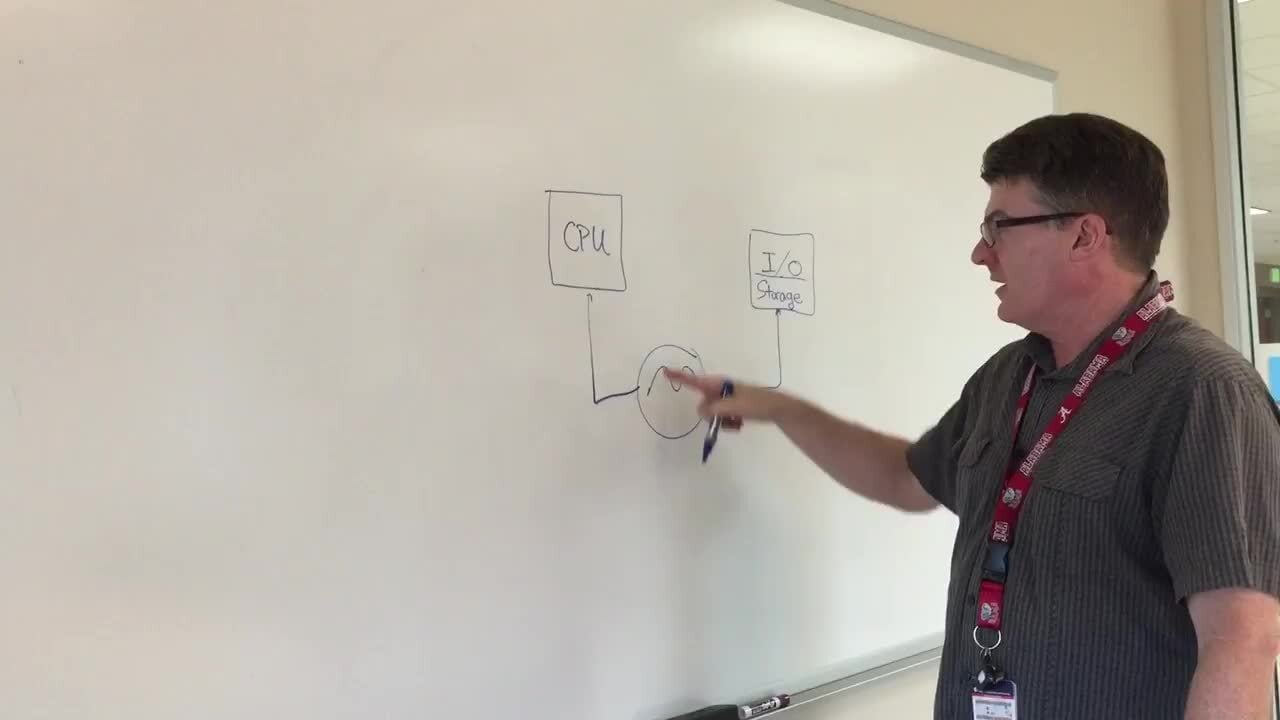
This is the first video in our PCIe series. In this video, we define PCIe architectures, focusing on common and separate clock architectures. Watch the rest of the video series below where Ron will cover the impact of different timing architectures.
Watch the Video Series Below