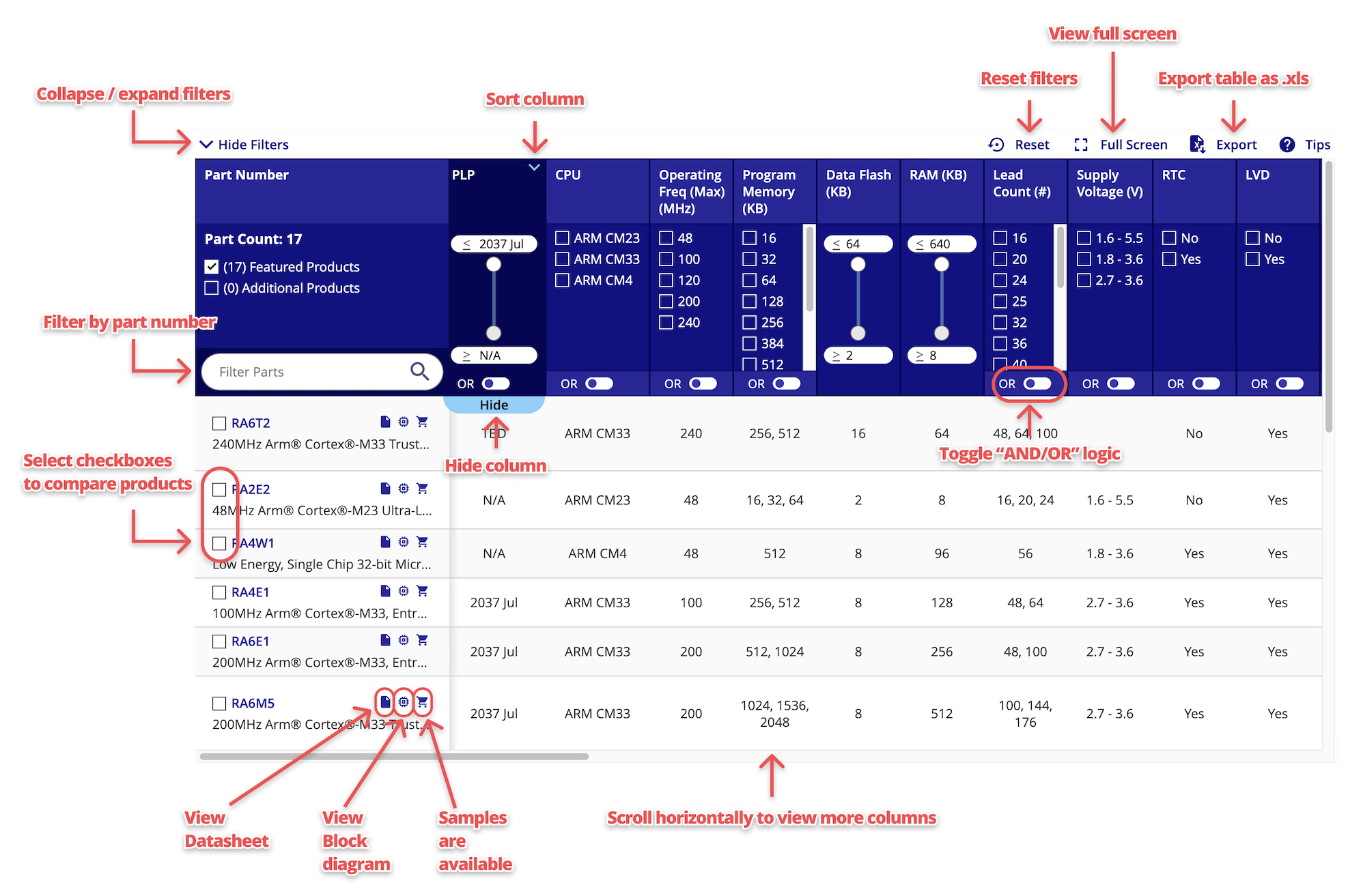
Image


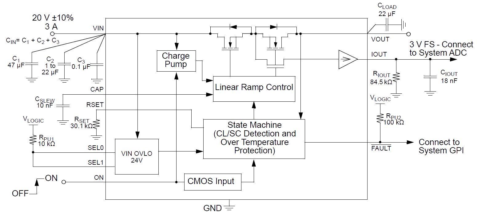
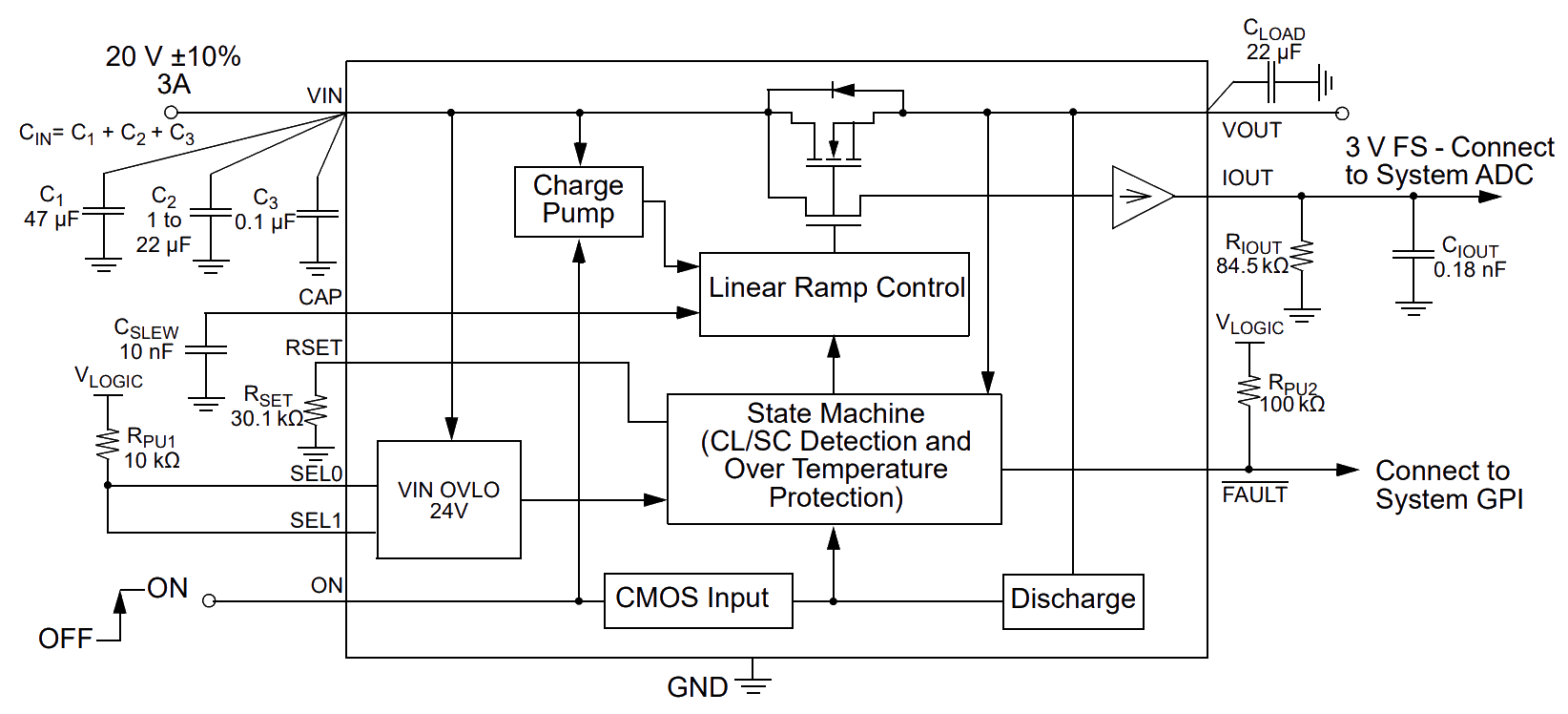
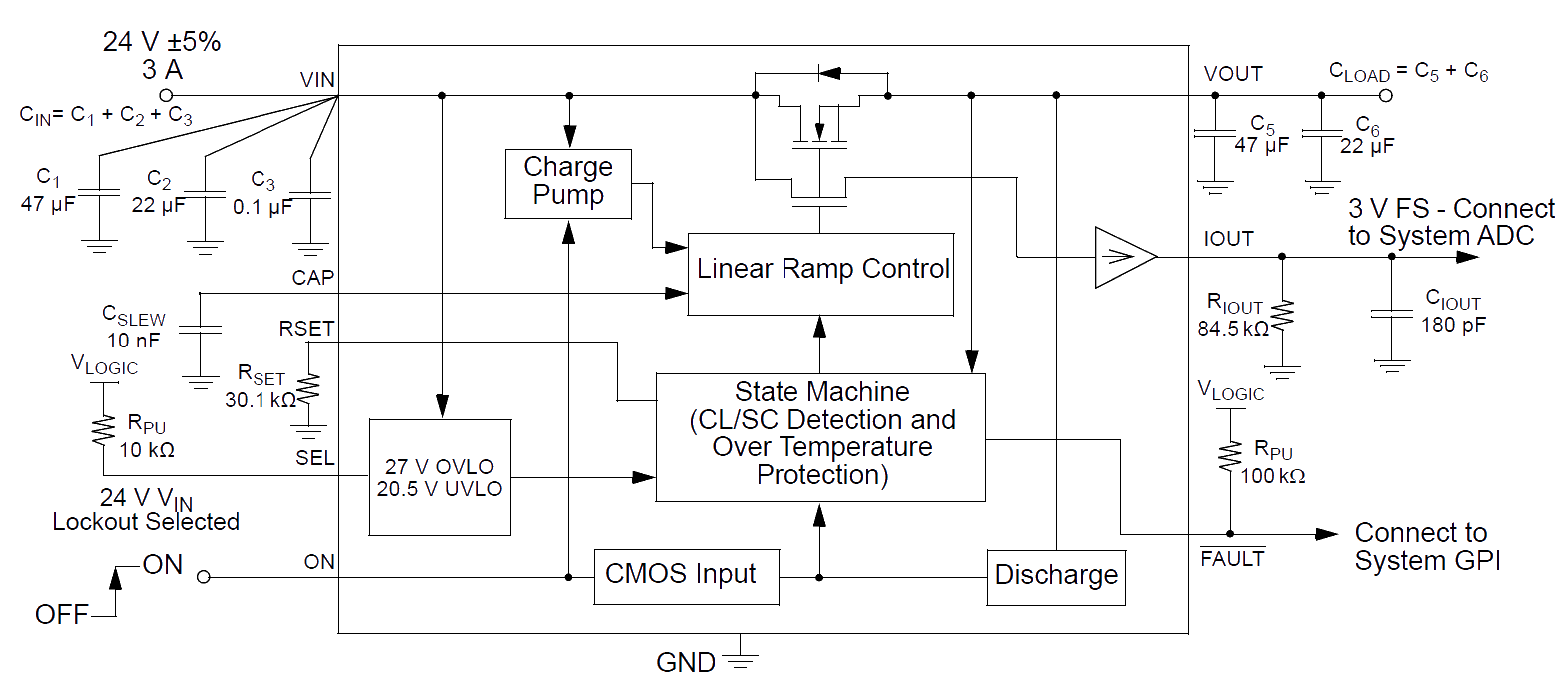
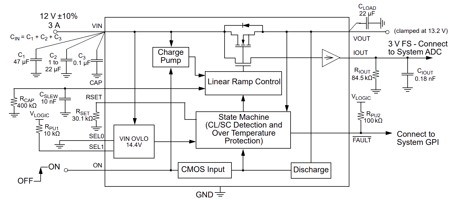
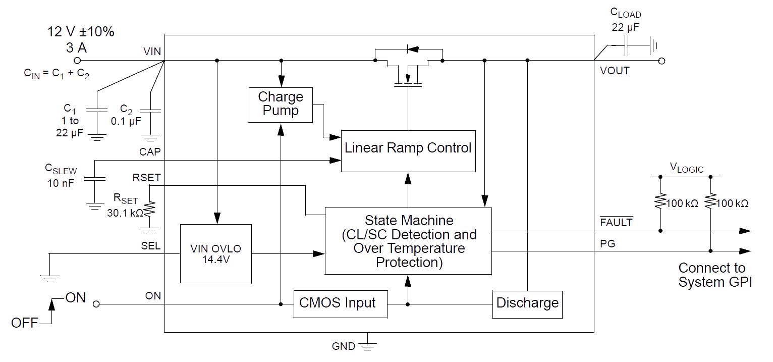
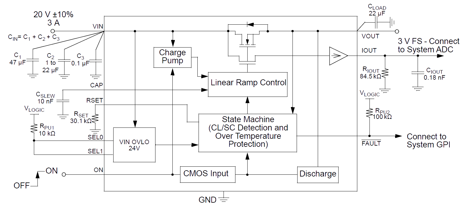
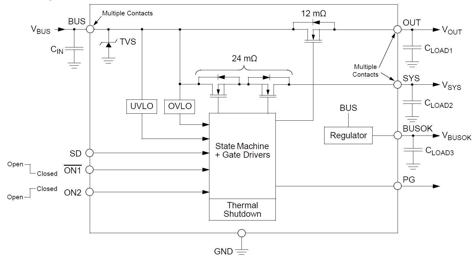
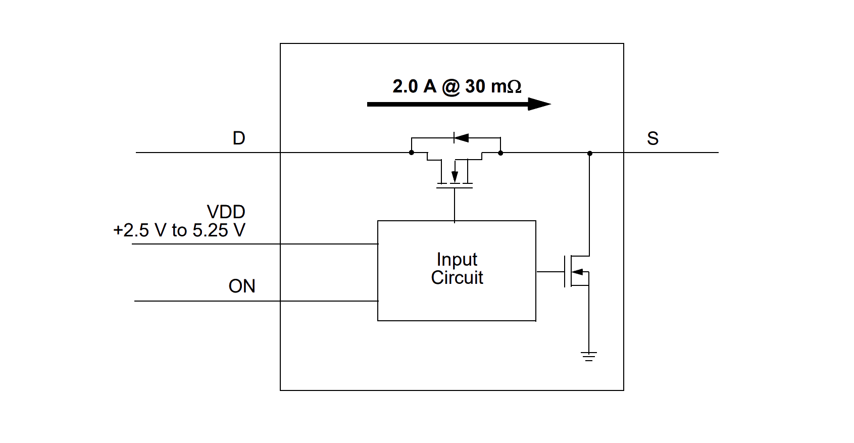
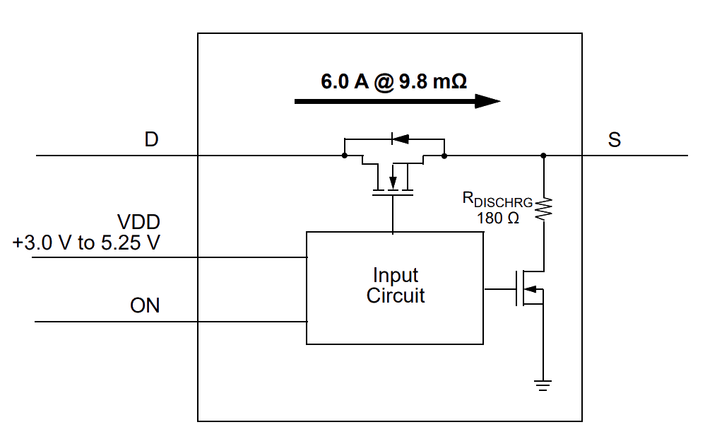
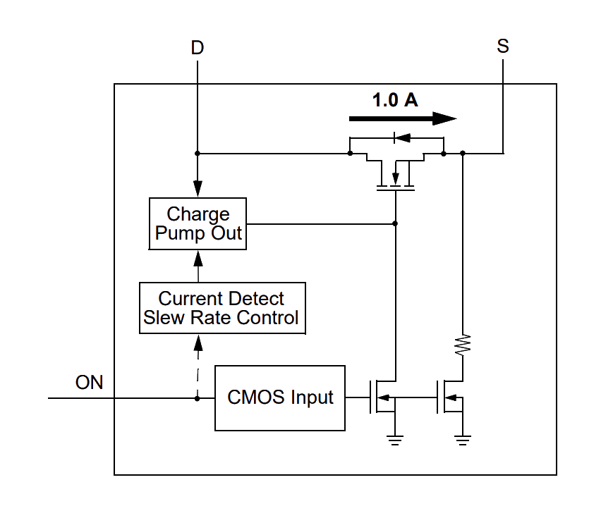
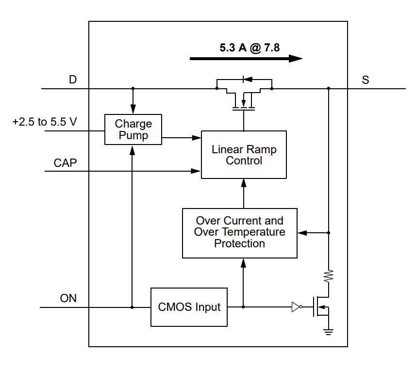
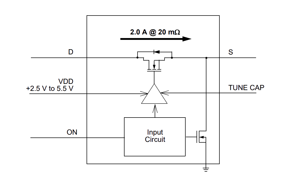
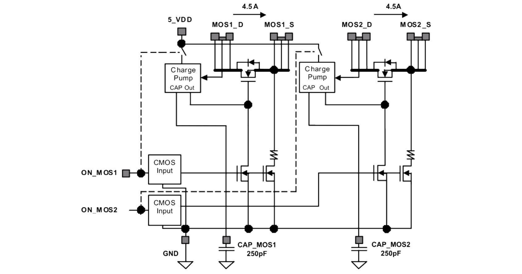
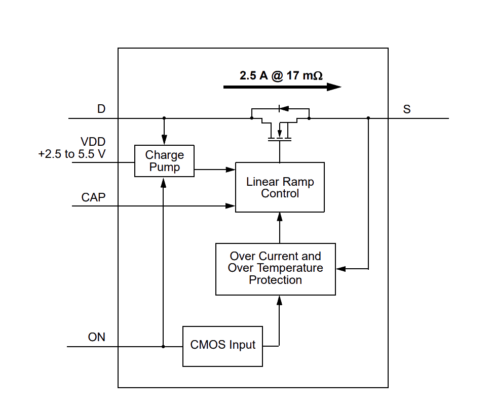
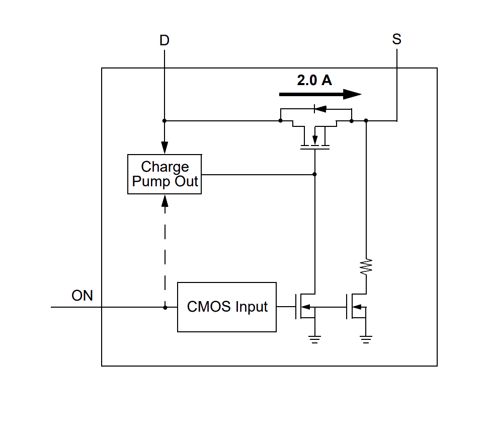
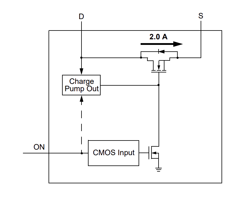
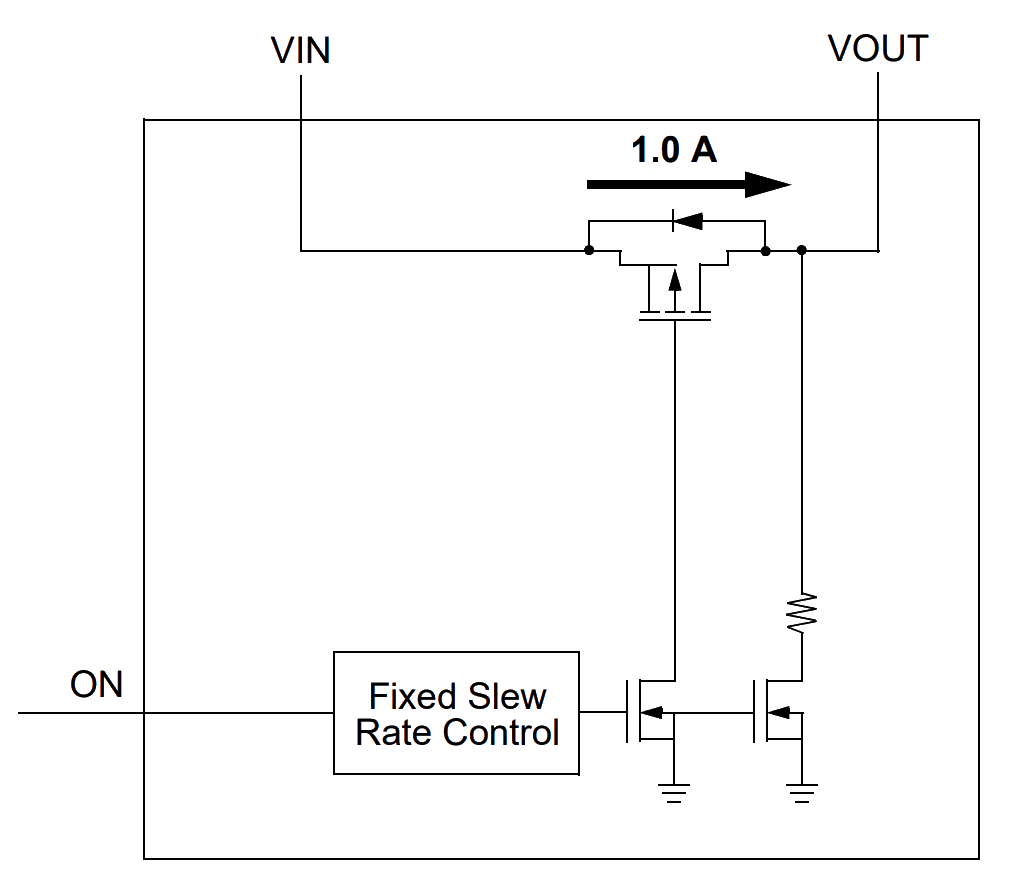
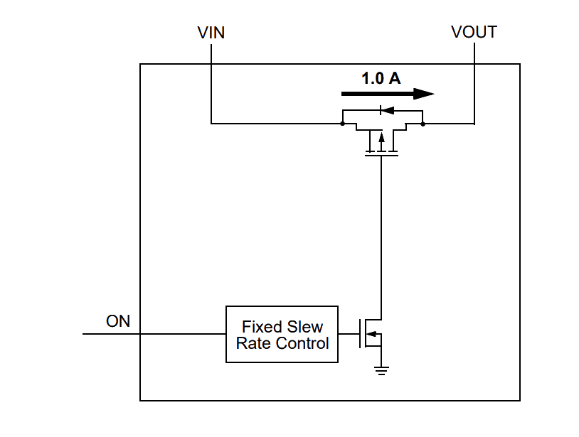
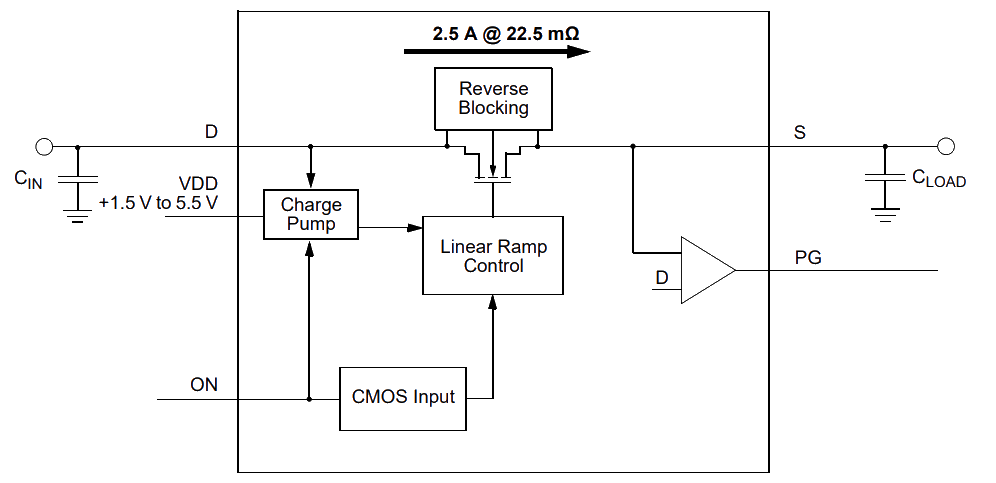
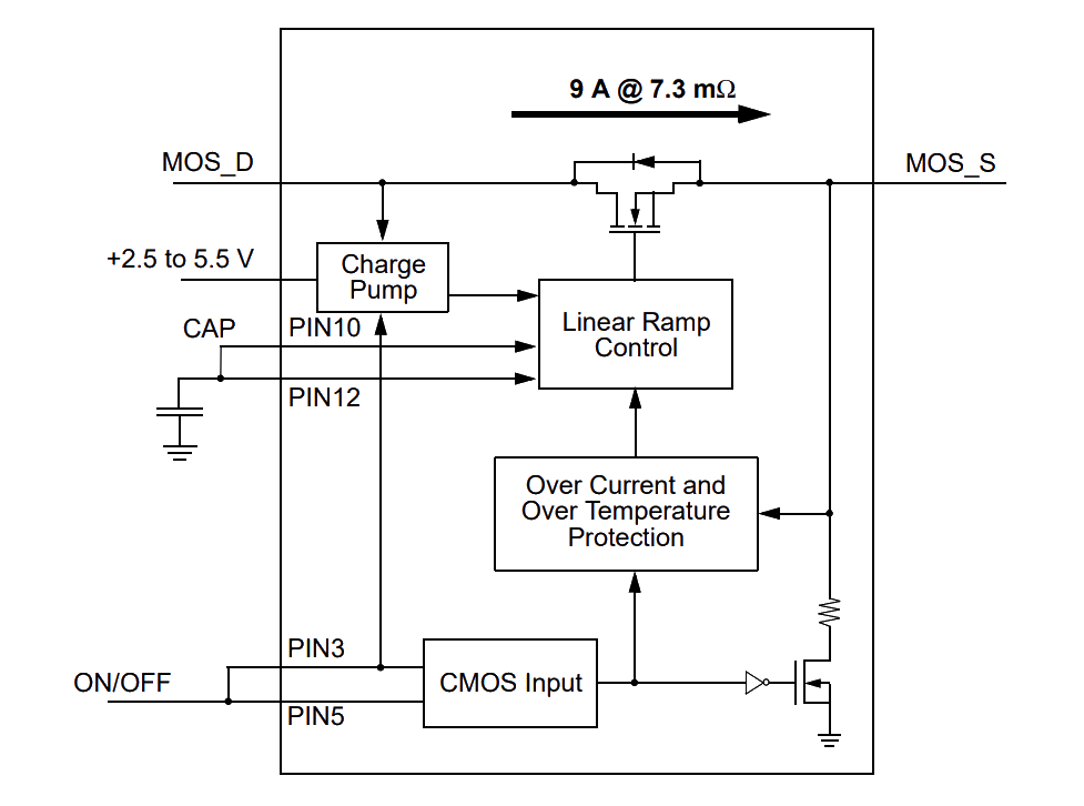
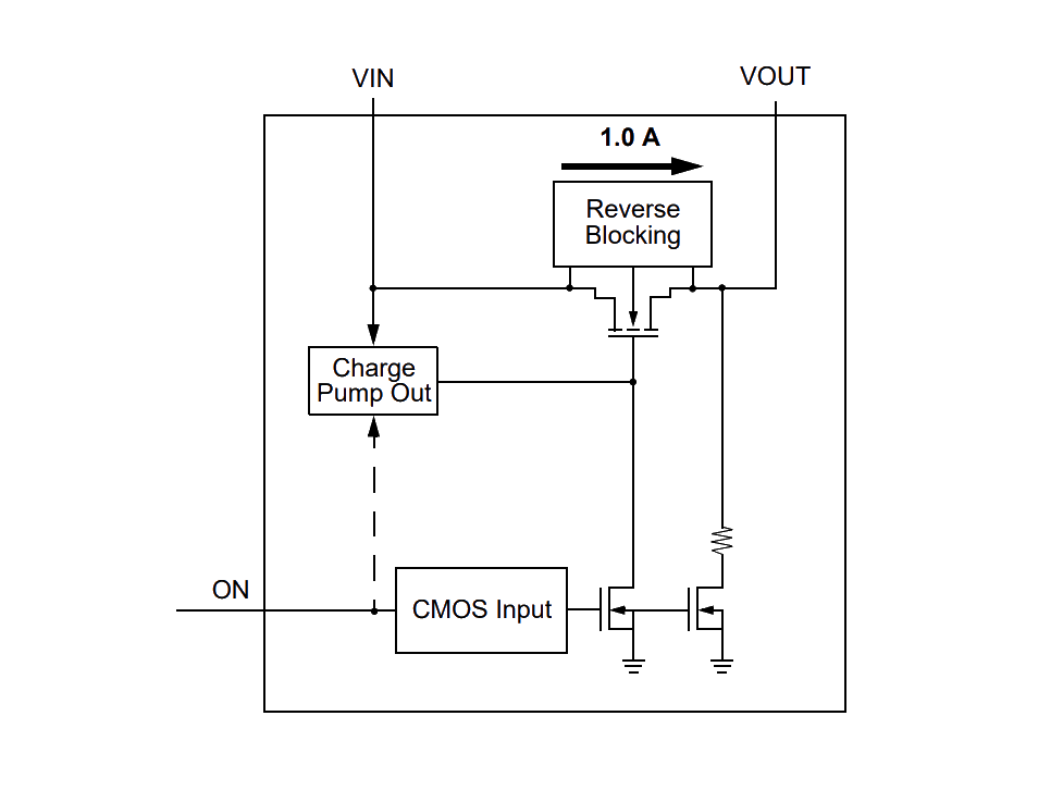
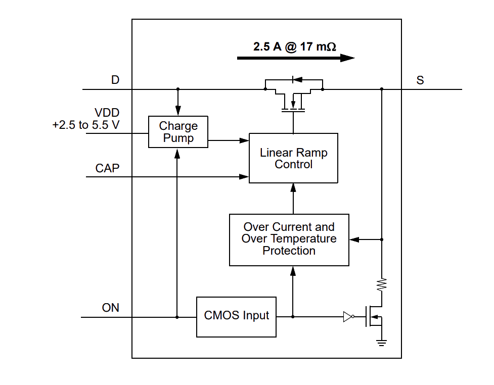
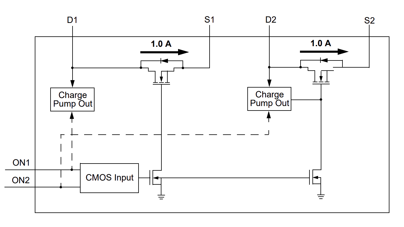
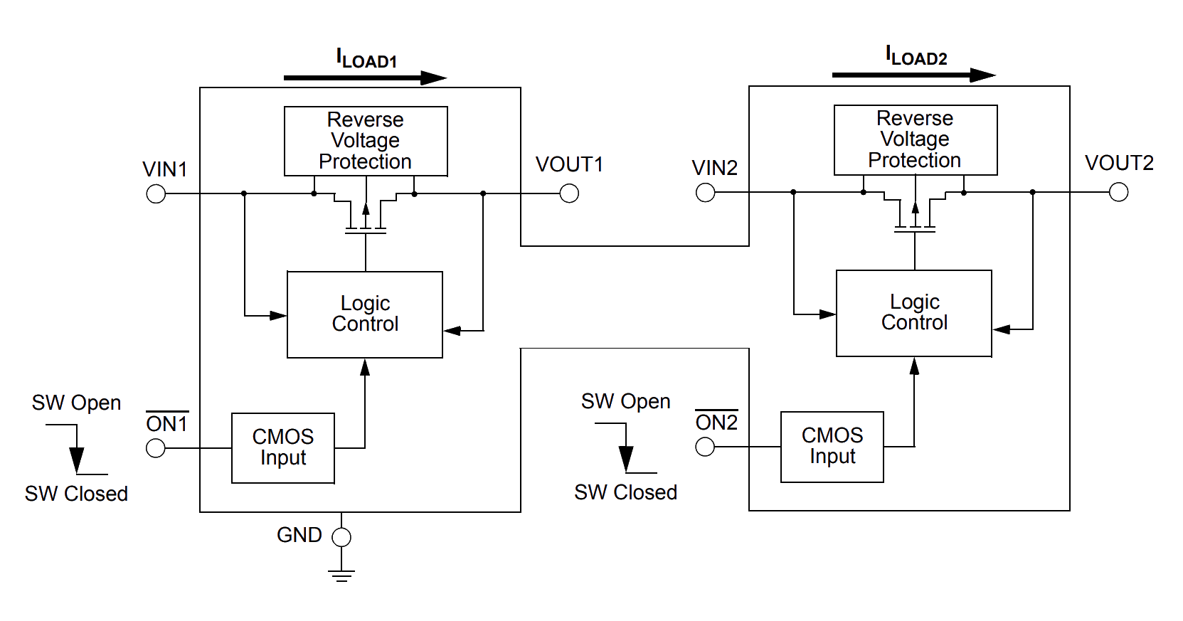
GreenFET high‑performance load switches are designed and optimized for high‑side power rail control applications from 0.25V to 25.2V where the load currents range from 1A to 9A.
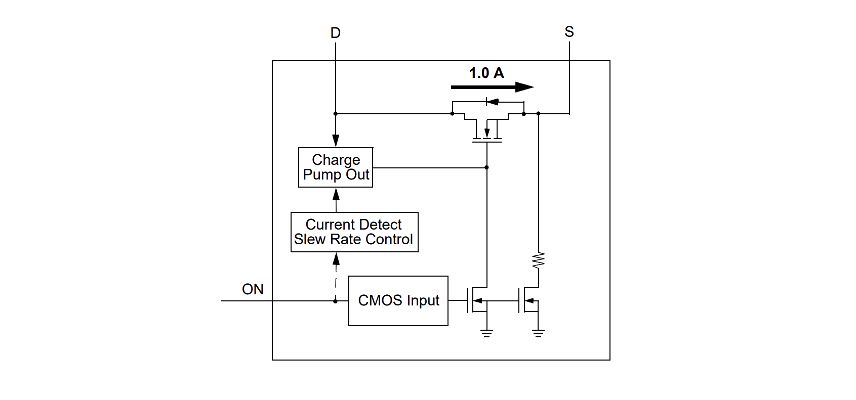
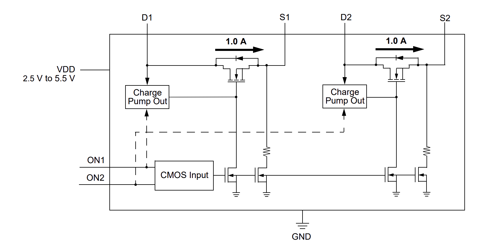
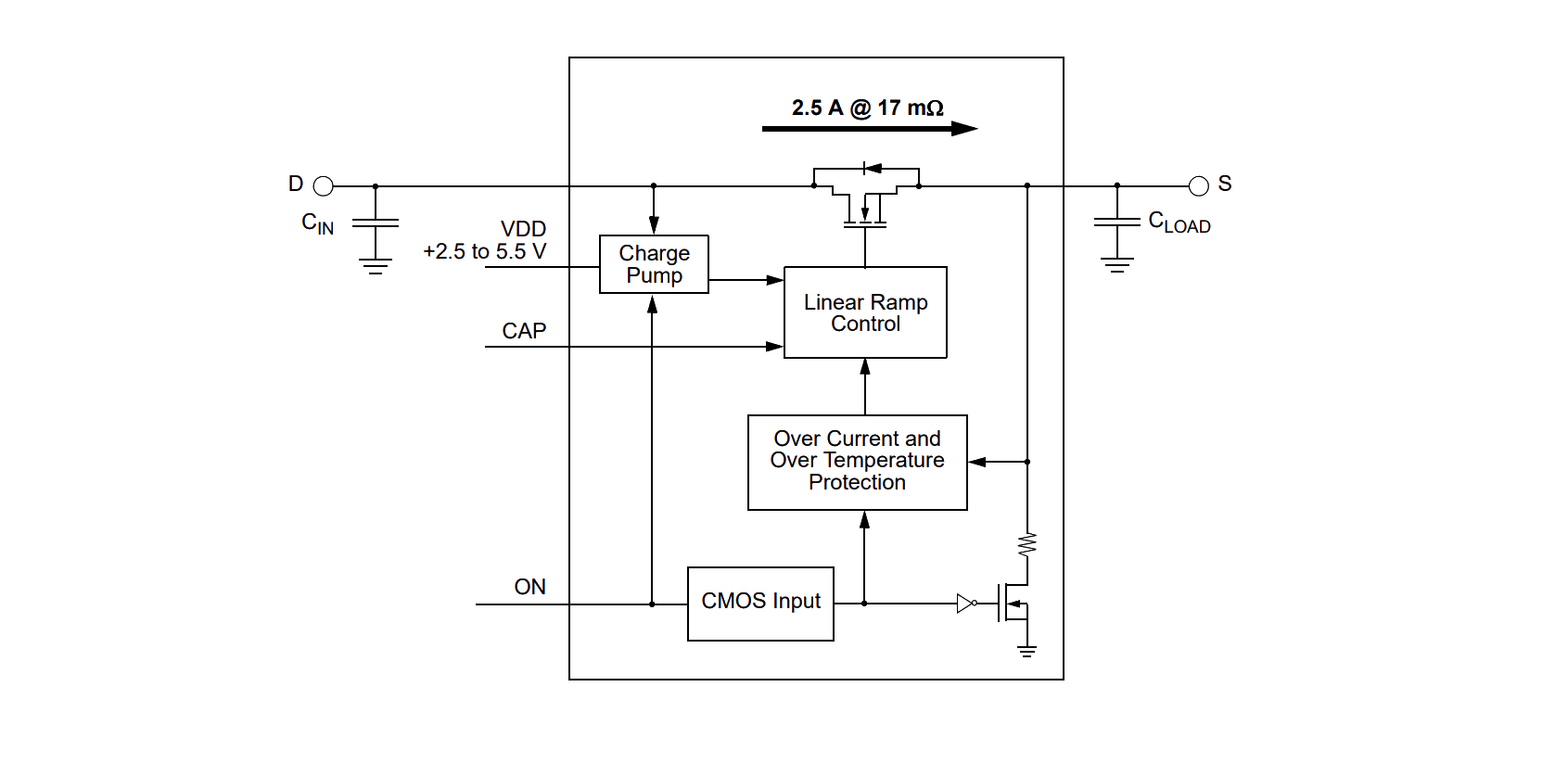
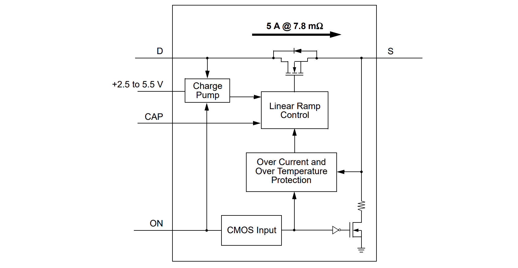
Using a proprietary MOSFET design, all GreenFET load switches achieve ultra‑stable RDSON across wide input and supply voltage ranges. Combining proprietary MOSFET IP and advanced assembly techniques, these advanced state‑of‑the‑art products are available in ultra‑small PCB footprints from 0.56mm² to 5.04mm² and exhibit low thermal resistances for high‑current operation.
Compared to discrete FET circuit implementations, GreenFET products combine high‑performance nFET or pFET structures, high current handling capability, charge pumps, as well as multiple protection and control circuits into space‑efficient single- and dual‑channel products. The combination of all these advanced features directly results in BOM (bill‑of‑material) component and cost reductions as well as increasing system reliability and reduced board size.
All low- and high‑voltage GreenFET load switches are designed and fully characterized over the commercial (0 °C to 70 °C), extended commercial (-20 °C to 70 °C), industrial (-40 °C to 85 °C), or extended industrial (-40 °C to 125 °C) temperature ranges. Consistent with generating very low thermal gradients, Renesas load switches are available in low thermal resistance, STDFN/STQFN RoHS‑compliant packaging, and wafer‑level chip scale packaging (WLCSP).
FET Pass Device Type |
VDD min. (V) |
VDD max. (V) |
VIN Channel 1 min. (V) |
VIN Channel 1 max. (V) |
VIN Channel 2 min. (V) |
VIN Channel 2 max. (V) |
RDSON (Typ) Channel 1 (mΩ) |
RDSON (Typ) Channel 2 (mΩ) |
IDS Channel 1 (A) |
IDS Channel 2 (A) |
Pkg. Type |
Enable |
Output Voltage Slew Rate set by |
Discharge Circuit |
Undervoltage Protection |
Over Voltage Protection |
Power Good (PG), FAULT indicator |
Reverse current blocking |
Reverse voltage detection |
Over Current Protection (OCP) |
Over Current Protection Setting Range Channel 1 |
Over Current Protection Setting Range Channel 2 |
Short Circuit Protection |
Over Temperature Protection (OTP) |
Current Monitor Output |
Internal TVS Surge Protection |
Temp. Range |
|
|---|---|---|---|---|---|---|---|---|---|---|---|---|---|---|---|---|---|---|---|---|---|---|---|---|---|---|---|---|
| Part Number | ||||||||||||||||||||||||||||
| High Voltage GreenFET Load Switch | Single N-Channel | 4.5 | 22 | 50 | 3 | STQFN-18 | Active High | Capacitor | No | Yes | Yes | FAULT | Yes | No | Adjustable | 1 - 3 | Yes | Yes | Yes | No | -40 to +85°C | |||||||
| High Voltage GreenFET Load Switch | Single N-Channel | 4.5 | 22 | 13.1 | 5 | STQFN-18 | Active High | Capacitor | Yes | Yes | Yes | FAULT | No | No | Adjustable | 1 - 5 | Yes | Yes | Yes | No | -40 to +85°C | |||||||
| High Voltage GreenFET Load Switch | Single N-Channel | 10.8 | 25.2 | 13.3 | 4 | STQFN-18 | Active High | Capacitor | Yes | Yes | Yes | FAULT | No | No | Adjustable | 1 - 4.5 | Yes | Yes | Yes | No | -40 to +85°C | |||||||
| High Voltage GreenFET Load Switch | Single N-Channel | 4.5 | 22 | 13.1 | 4 | STQFN-18 | Active High | Capacitor | Yes | Yes | Yes | FAULT | No | No | Adjustable | 1 - 4.5 | Yes | Yes | Yes | No | -40 to +85°C | |||||||
| High Voltage GreenFET Load Switch | Single N-Channel | 10.8 | 25.2 | 13.3 | 5 | STQFN-18 | Active High | Capacitor | Yes | Yes | Yes | FAULT | No | No | Adjustable | 1 - 5 | Yes | Yes | Yes | No | -40 to +85°C | |||||||
| High Voltage GreenFET Load Switch | Single N-Channel | 4.5 | 22 | 13.1 | 6 | STQFN-18 | Active High | Capacitor | Yes | Yes | Yes | FAULT | No | No | Adjustable | 1 - 7 | Yes | Yes | Yes | No | -40 to +85°C | |||||||
| High Voltage GreenFET Load Switch | Single N-Channel | 10.8 | 25.2 | 13.3 | 3.5 | STQFN-18 | Active High | Capacitor | Yes | Yes | Yes | FAULT | No | No | Adjustable | 1 - 4 | Yes | Yes | Yes | No | -40 to +125°C | |||||||
| High Voltage GreenFET Load Switch | Single N-Channel | 4.5 | 22 | 13.1 | 3.5 | STQFN-18 | Active High | Capacitor | Yes | Yes | Yes | FAULT | No | No | Adjustable | 1 - 4 | Yes | Yes | Yes | No | -40 to +125°C | |||||||
| High Voltage GreenFET Load Switch | Single N-Channel | 10.8 | 25.2 | 13.3 | 4 | STQFN-18 | Active High | Capacitor | Yes | Yes | Yes | FAULT | No | No | Adjustable | 1 - 4.5 | Yes | Yes | Yes | No | -40 to +85°C | |||||||
| High Voltage GreenFET Load Switch | Single N-Channel | 4.5 | 25.2 | 13 | 5 | STQFN-18 | Active High | Capacitor | Yes | Yes | No | FAULT | No | No | Adjustable | 1 - 5 | Yes | Yes | Yes | No | -40 to +85°C | |||||||
| High Voltage GreenFET Load Switch | Single N-Channel | 4.5 | 20 | 50 | 3 | STQFN-18 | Active High | Capacitor | No | No | Yes | FAULT | Yes | No | Adjustable | 1 - 3 | Yes | Yes | Yes | No | -40 to +85°C | |||||||
| High Voltage GreenFET Load Switch | Single N-Channel | 4.5 | 13.2 | 18 | 5 | STQFN-18 | Active High | Capacitor | Yes | Yes | Yes | FAULT | No | No | Adjustable | 1 - 5 | Yes | Yes | Yes | No | -40 to +85°C | |||||||
| High Voltage GreenFET Load Switch | Single N-Channel | 4.5 | 13.2 | 18 | 6 | STQFN-18 | Active High | Capacitor | Yes | Yes | Yes | FAULT | No | No | Adjustable | 1 - 7 | Yes | Yes | Yes | No | -40 to +85°C | |||||||
| High Voltage GreenFET Load Switch | Single N-Channel | 4.5 | 13.2 | 15 | 4 | STQFN-18 | Active High | Capacitor | Yes | Yes | Yes | PG & FAULT | No | No | Adjustable | 1 - 5 | Yes | Yes | No | No | -40 to +85°C | |||||||
| High Voltage GreenFET Load Switch | Single N-Channel | 4.5 | 22 | 13.1 | 5 | STQFN-18 | Active High | Capacitor | Yes | Yes | Yes | FAULT | No | No | Adjustable | 1 - 5 | Yes | Yes | Yes | No | -40 to +85°C | |||||||
| High Voltage GreenFET Load Switch | Power Splitter | 2.7 | 13.3 | 2.7 | 4.9 | 12 | 24 | 6 | 6 | WLCSP-28 | OUT: Active Low SYS: Active High | No | No | Yes | Yes | OUT: No SYS: PG | No, OUT: No SYS: Yes | No | No | No | No | No | Yes | -40 to +85°C | ||||
| High Voltage GreenFET Load Switch | Single N-Channel | 2.5 | 20 | 23 | 4.5 | WLCSP-12 | Active Low | No | No | No | Yes | PG | No | No | Internally Fixed | 7 | Yes | Yes | No | Yes | -40 to +85°C | |||||||
| High Voltage GreenFET Load Switch | Single N-Channel | 2.5 | 5.5 | 70 | 1.3 | WLCSP-9 | Active High | Internally Fixed | No | Yes | Yes | FAULT | Yes | Yes | Adjustable | 0.16 - 1.62 | No | Yes | No | No | -40 to +85°C | |||||||
| High Voltage GreenFET Load Switch | Single N-Channel | 2.7 | 5.5 | 70 | 1.5 | WLCSP-9 | Active Low | Internally Fixed | No | Yes | Yes | FAULT | Yes | Yes | Adjustable | 0.16 - 1.81 | No | Yes | No | No | -40 to +85°C | |||||||
| High Voltage GreenFET Load Switch | Power MUX | 2.8 | 6 | 2.8 | 6 | 52 | 52 | 3 | 3 | WLCSP-20 | No | Capacitor | No | Yes | Yes | No | Yes | Yes | Adjustable | 1.3 - 3.5 | 1.3 - 3.5 | Yes | Yes | No | No | -40 to +85°C | ||
| High Voltage GreenFET Load Switch | Power MUX | 2.8 | 22 | 2.8 | 22 | 52 | 52 | 3 | 3 | WLCSP-20 | No | Capacitor | No | Yes | Yes | No | Yes | Yes | Adjustable | 1.3 - 3.5 | 1.3 - 3.5 | Yes | Yes | No | No | -40 to +85°C | ||
| High Voltage GreenFET Load Switch | Power MUX | 4 | 5.5 | 4 | 13.2 | 40 | 67 | 3 | 1.25 | FC-QFN-12 | Active High | Internally Fixed | Yes | Yes | Yes | FAULT | Yes | Yes | Adjustable | 0.65 - 4.08 | 0.5 - 1.9 | Yes | Yes | No | No | -20 to +85°C | ||
| GreenFET Single N-Channel Load Switch | Single N-Channel | 2.5 | 5.5 | 40 | 1 | STDFN-4 | Active High | Resistor | Yes | No | No | No | No | No | No | No | Yes | No | No | -40 to +85°C | ||||||||
| GreenFET Dual N-Channel Load Switch | Dual N-Channel | 2.5 | 5.5 | 0.85 | 5.5 | 0.85 | 5.5 | 40 | 40 | 1 | 1 | STDFN-8 | Active High | Resistor | Yes | No | No | No | No | No | No | No | Yes | No | No | -40 to +85°C | ||
| GreenFET Single N-Channel Load Switch | Single N-Channel | 2.5 | 5.5 | 0.9 | 5.5 | 17 | 2.5 | STDFN-8 | Active High | Capacitor | Yes | No | No | No | No | No | Internally Fixed | 3.7 | Yes | Yes | No | No | -40 to +85°C | |||||
| GreenFET Single N-Channel Load Switch | Single N-Channel | 2.5 | 5.5 | 1 | 5.5 | 7.8 | 5 | TDFN-8 | Active High | Capacitor | Yes | No | No | No | No | No | Internally Fixed | 7 | Yes | Yes | No | No | -20 to +70°C | |||||
| GreenFET Single N-Channel Load Switch | Single N-Channel | 2.5 | 5.5 | 0.85 | 5.5 | 7.8 | 6 | TDFN-8 | Active High | Capacitor | Yes | No | No | No | No | No | Internally Fixed | 7 | Yes | Yes | No | No | -40 to +85°C | |||||
| GreenFET Single N-Channel Load Switch | Single N-Channel | 2.5 | 5.25 | 0.85 | 3.75 | 30 | 2 | STDFN-8 | Active High | No | Yes | No | No | No | No | No | No | No | No | No | No | -20 to +70°C | ||||||
| GreenFET Single N-Channel Load Switch | Single N-Channel | 3 | 5.25 | 0.85 | 3.75 | 9.8 | 6 | TDFN-9 | Active High | No | Yes | No | No | No | No | No | No | No | No | No | No | -40 to +85°C | ||||||
| GreenFET Single N-Channel Load Switch | Single N-Channel | 2.5 | 5.5 | 80 | 1 | STDFN-4 | Active High | Resistor | Yes | No | No | No | No | No | No | No | Yes | No | No | -20 to +70°C | ||||||||
| GreenFET Single N-Channel Load Switch | Single N-Channel | 2.5 | 5.5 | 0.85 | 5.5 | 7.8 | 5.3 | TDFN-8 | Active High | Capacitor | Yes | No | No | No | No | No | Internally Fixed | 7 | Yes | Yes | No | No | -40 to +85°C | |||||
| GreenFET Dual N-Channel Load Switch | Dual N-Channel | 2.5 | 5.5 | 0.85 | 5.5 | 0.85 | 5.5 | 80 | 80 | 1 | 1 | STDFN-8 | Active High | Resistor | Yes | No | No | No | No | No | No | No | Yes | No | No | -40 to +85°C | ||
| GreenFET Single N-Channel Load Switch | Single N-Channel | 2.5 | 5.5 | 0.85 | 3.75 | 20 | 2 | STDFN-8 | Active High | Capacitor | Yes | No | No | No | No | No | No | No | Yes | No | No | -40 to +85°C | ||||||
| GreenFET Dual N-Channel Load Switch | Dual N-Channel | 2.5 | 5.5 | 0.9 | 5.5 | 0.9 | 5.5 | 14.5 | 14.5 | 4.5 | 4.5 | STDFN-14 | Active High | Capacitor | Yes | No | No | No | No | No | Internally Fixed | 6 | 6 | Yes | Yes | No | No | -40 to +85°C |
| GreenFET Single N-Channel Load Switch | Single N-Channel | 2.5 | 5.5 | 0.85 | 5.5 | 17 | 2.5 | STDFN-8 | Active High | Capacitor | No | No | No | No | No | No | Internally Fixed | 3.7 | Yes | Yes | No | No | -20 to +70°C | |||||
| GreenFET Single N-Channel Load Switch | Single N-Channel | 0.85 | 1.9 | 15.5 | 2 | STDFN-4 | Active High | No | Yes | No | No | No | No | No | No | No | Yes | No | No | -40 to +85°C | ||||||||
| GreenFET Single N-Channel Load Switch | Single N-Channel | 0.85 | 1.9 | 15.5 | 2 | STDFN-4 | Active High | No | No | No | No | No | No | No | No | No | Yes | No | No | -40 to +85°C | ||||||||
| GreenFET Single P-Channel Load Switch | Single P-Channel | 1.5 | 5.5 | 28.5 | 1 | STDFN-4 | Active High | Internally Fixed | Yes | No | No | No | No | No | No | No | No | No | No | -40 to +85°C | ||||||||
| GreenFET Single P-Channel Load Switch | Single P-Channel | 1.5 | 5.5 | 28.5 | 1 | STDFN-4 | Active High | Internally Fixed | No | No | No | No | No | No | No | No | No | No | No | -40 to +85°C | ||||||||
| GreenFET Single N-Channel Reverse Blocking Load Switch | Single N-Channel | 1.5 | 5.5 | 1 | 5.5 | 22.5 | 2.5 | STDFN-8 | Active High | Internally Fixed | No | No | No | PG | Yes | No | No | No | Yes | No | No | -40 to +85°C | ||||||
| GreenFET Single N-Channel Load Switch | Single N-Channel | 2.5 | 5.5 | 1 | 5.5 | 7.3 | 9 | STDFN-14 | Active High | Capacitor | Yes | No | No | No | No | No | Internally Fixed | 12 | Yes | Yes | No | No | -40 to +85°C | |||||
| GreenFET Single N-Channel Reverse Blocking Load Switch | Single N-Channel | 0.85 | 1.9 | 14.6 | 1 | STDFN-4 | Active High | No | Yes | No | No | No | Yes | No | No | No | Yes | No | No | -40 to +85°C | ||||||||
| GreenFET Single N-Channel Load Switch | Single N-Channel | 2.5 | 5.5 | 0.85 | 5.5 | 17 | 2.5 | STDFN-8 | Active High | Capacitor | Yes | No | No | No | No | No | Internally Fixed | 3.7 | Yes | Yes | No | No | -40 to +85°C | |||||
| GreenFET Dual N-Channel Load Switch | Dual N-Channel | 2.5 | 5.5 | 0.85 | 5.5 | 0.85 | 5.5 | 40 | 40 | 1 | 1 | STDFN-8 | Active High | Resistor | No | No | No | No | No | No | No | No | Yes | No | No | -40 to +85°C | ||
| GreenFET Single N-Channel Reverse Blocking Load Switch | Single N-Channel | 2.5 | 5.5 | 0.85 | 5.5 | 7.8 | 9 | STDFN-14 | Active High | Capacitor | Yes | No | No | No | Yes | No | No | No | Yes | No | No | -40 to +85°C | ||||||
| GreenFET Dual N-Channel Load Switch | Dual N-Channel | 2.5 | 5.5 | 0.85 | 5.5 | 0.85 | 5.5 | 16 | 16 | 4.5 | 4.5 | STDFN-14 | Active High | Capacitor | Yes | No | No | No | Yes | No | No | No | Yes | No | No | -40 to +85°C | ||
| GreenFET Dual N-Channel Load Switch | Dual N-Channel | 2.5 | 5.5 | 0.85 | 5.5 | 0.85 | 5.5 | 16 | 16 | 4.5 | 4.5 | STDFN-14 | Active High | Capacitor | No | No | No | No | Yes | No | No | No | Yes | No | No | -40 to +85°C | ||
| GreenFET Single N-Channel Load Switch | Single N-Channel | 2.5 | 5.5 | 0.85 | 5.5 | 8.5 | 4 | TDFN-8 | Active High | Capacitor | Yes | No | No | No | No | No | Internally Fixed | 6 | Yes | Yes | No | No | -40 to +85°C | |||||
| GreenFET Dual P-Channel Reverse Blocking Load Switch | Dual P-Channel | 1.5 | 5.5 | 1.5 | 5.5 | 45 | 45 | 2 | 2 | STDFN-8 | Active High | No | No | Yes | No | No | Yes | Yes | No | No | No | No | No | -40 to +85°C | ||||
| GreenFET Dual P-Channel Reverse Blocking Load Switch | Dual P-Channel | 1.5 | 5.5 | 1.5 | 5.5 | 45 | 45 | 2 | 2 | STDFN-8 | Active Low | No | No | Yes | No | No | Yes | Yes | No | No | No | No | No | -40 to +85°C |
|
|
|
|
|---|---|---|
| Type | Title | Date |
| PCB Design Files | ZIP 65 KB | |
| PCB Design Files | ZIP 9 KB | |
| PCB Design Files | ZIP 221 KB | |
| PCB Design Files | ZIP 23 KB | |
| PCB Design Files | ZIP 2 KB | |
| PCB Design Files | ZIP 61 KB | |
6 items
|
||
| Blog Post | Jul 1, 2023 |
