Overview
Description
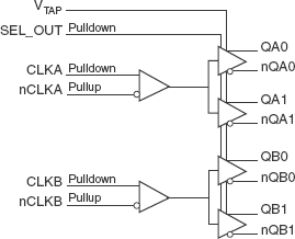
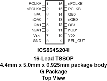
The 854S204I is a low skew, high performance dual, programmable 1-to-2 Differential-to-LVDS, LVPECL Fanout Buffer. The PCLKx, nPCLKx pairs can accept most standard differential input levels. With the selection of SEL_OUT signal, outputs can be selected be to either LVDS or LVPECL levels. The 854S204I is characterized to operate from either a 2.5V or a 3.3V power supply. Guaranteed output and bank skew characteristics make the 854S204I ideal for those clock distribution applications demanding well defined performance and repeatability. The 854S204I is a low skew, high performance dual, programmable 1-to-2 Differential-to-LVDS, LVPECL Fanout Buffer. The PCLKx, nPCLKx pairs can accept most standard differential input levels. With the selection of SEL_OUT signal, outputs can be selected be to either LVDS or LVPECL levels. The 854S204I is characterized to operate from either a 2.5V or a 3.3V power supply. Guaranteed output and bank skew characteristics make the 854S204I ideal for those clock distribution applications demanding well defined performance and repeatability.
Features
- Two programmable differential LVDS or LVPECL output banks
- Two differential clock input pairs
- PCLKx, nPCLKx pairs can accept the following differential input levels: LVDS, LVPECL, SSTL, CML
- Maximum output frequency: 3GHz
- Translates any single ended input signal to LVDS levels with resistor bias on nPCLKx inputs
- Output skew: 15ps (maximum)
- Bank skew: 15ps (maximum)
- Propagation delay: 500ps (maximum)
- Additive phase jitter, RMS: 0.15ps (typical)
- Full 3.3V or 2.5V supply modes
- -40°C to 85°C ambient operating temperature
- Available in lead-free (RoHS 6) package
Comparison
Applications
Design & Development
Models
ECAD Models
Schematic symbols, PCB footprints, and 3D CAD models from SamacSys can be found by clicking on products in the Product Options table. If a symbol or model isn't available, it can be requested directly from the website.

| TSSOP | 16 | I | Yes | Tube | ||
| TSSOP | 16 | I | Yes | Reel |

Tips for Using This Parametric Table:
- Hide Filters button in header: Collapse or expands filters
- Column sort buttons in header: Sort Column alphabetically / numerically descending or ascending
- Reset button in header: Reset all filters to the page default
- Full Screen button in header: Expand the table to full screen view (user must close out of full screen before they can interact with rest of page)
- Export button in header: Export the filtered results of the table to an Excel document
- Filter parts search bar in header: Type to filter table results by part number
- Hide column button in column headers: Select to hide columns in table
- AND / OR toggle switches in header: Toggles the logic of this particular filter to be “AND” or “OR” logic for filtering results
- Multiselect checkboxes at beginning of each row in table: Select these checkboxes to compare products against each other
- Document icon next to product name in row: View the featured document for this product
- Chip icon next to the right of the document icon in row: View the block diagram for this product
- Cart icon to the right of the chip icon: Indicates that samples are available for this product