Overview
Description
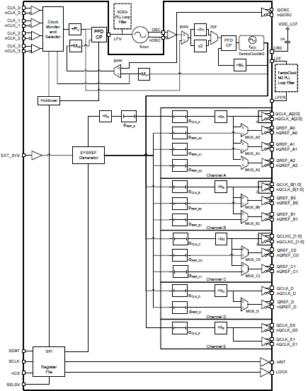
The 8V19N490-24 is a fully integrated FemtoClock® NG jitter attenuator and clock synthesizer designed as a high-performance clock solution for conditioning and frequency/phase management of wireless base station radio equipment boards. The device is optimized to deliver excellent phase noise performance as required in GSM, WCDMA, LTE, and LTE-A radio board implementations. The device supports JESD204B subclass 0 and 1 clocks.
A two-stage PLL architecture supports both jitter attenuation and frequency multiplication. The first stage PLL is the jitter attenuator and uses an external VCXO for best possible phase noise characteristics. The second stage PLL locks on the VCXO-PLL output signal and synthesizes the target frequency.
The device supports the clock generation of high-frequency clocks from the selected VCO and low-frequency synchronization signals (SYSREF). SYSREF signals are internally synchronized to the clock signals. Delay functions exist for achieving alignment and controlled phase delay between system reference and clock signals and to align/delay individual output signals. The four redundant inputs are monitored for activity. Four selectable clock switching modes are provided to handle clock input failure scenarios. Auto-lock, individually programmable output frequency dividers, and phase adjustment capabilities are added for flexibility. The device is configured through a 3-wire SPI interface and reports lock and signal loss status in internal registers and via a lock detect (LOCK) output. Internal status bit changes can also be reported via the nINT output. The 8V19N490-24 is ideal for driving converter circuits in wireless infrastructure, radar/imaging, and instrumentation/medical applications.
For information regarding evaluation boards and material, please contact your local sales representative.
Features
- High-performance clock RF-PLL with support for JESD204B
- Optimized for low-phase noise: -150dBc/Hz (800kHz offset; 245.76MHz clock)
- Integrated phase noise of 57fs RMS typical (12kHz–20MHz)
- Dual-PLL architecture
- First PLL stage with external VCXO for clock jitter attenuation
- Second PLL with internal FemtoClock NG PLL: 2457.6MHz
- For 3932.16MHz: see 8V19N492-39
- For 3686.4MHz: see 8V19N491-36
- For 2949.12MHz: see 8V19N490A and 8V19N492
- For 1966.08MHz: see 8V19N490-19
- Six output channels with a total of 19 outputs, organized in:
- Four JESD204B channels (device clock and SYSREF output) with two, four and six outputs
- One clock channel with two outputs
- One VCXO output
- Configurable integer clock frequency dividers
- Supported clock output frequencies include: 2457.6, 1228.8, 614.4, 491.52, 307.2, 153.6, 122.88
- Low-power LVPECL/LVDS outputs support configurable signal amplitude, DC and AC coupling and LVPECL, LVDS line terminations techniques
- Phase delay circuits:
- Clock phase delay with 256 steps of 407ps and a range of 0 to 103.76ns
- Individual SYSREF phase delay with 8 steps of 203ps
- Additional individual SYSREF fine phase delay with 25ps steps
- Global SYSREF signal delay with 256 steps of 407ps and a range of 0 to 103.76ns
- Redundant input clock architecture with four inputs, including:
- Input activity monitoring
- Manual and automatic, fault-triggered clock selection modes
- Priority controlled clock selection
- Digital holdover and hitless switching
- Differential inputs accept LVDS and LVPECL signals
- SYSREF generation modes include internal and external trigger mode for JESD204B
- Supply voltage: 3.3V
- SPI and control I/O voltage: 1.8V/3.3V (selectable)
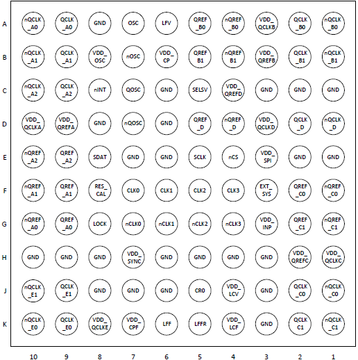
- Package: 11 x 11 mm 100-CABGA
Comparison
Applications
Design & Development
Software & Tools
Models
ECAD Models
Schematic symbols, PCB footprints, and 3D CAD models from SamacSys can be found by clicking on products in the Product Options table. If a symbol or model isn't available, it can be requested directly from the website.

| CABGA | 100 | I | Yes | Tray | 3 | 17.56 | Get Samples, | |
| CABGA | 100 | I | Yes | Reel | 3 |

Tips for Using This Parametric Table:
- Hide Filters button in header: Collapse or expands filters
- Column sort buttons in header: Sort Column alphabetically / numerically descending or ascending
- Reset button in header: Reset all filters to the page default
- Full Screen button in header: Expand the table to full screen view (user must close out of full screen before they can interact with rest of page)
- Export button in header: Export the filtered results of the table to an Excel document
- Filter parts search bar in header: Type to filter table results by part number
- Hide column button in column headers: Select to hide columns in table
- AND / OR toggle switches in header: Toggles the logic of this particular filter to be “AND” or “OR” logic for filtering results
- Multiselect checkboxes at beginning of each row in table: Select these checkboxes to compare products against each other
- Document icon next to product name in row: View the featured document for this product
- Chip icon next to the right of the document icon in row: View the block diagram for this product
- Cart icon to the right of the chip icon: Indicates that samples are available for this product
Videos & Training
News & Blog Posts
| Blog Post | Apr 27, 2021 |
