Overview
Description
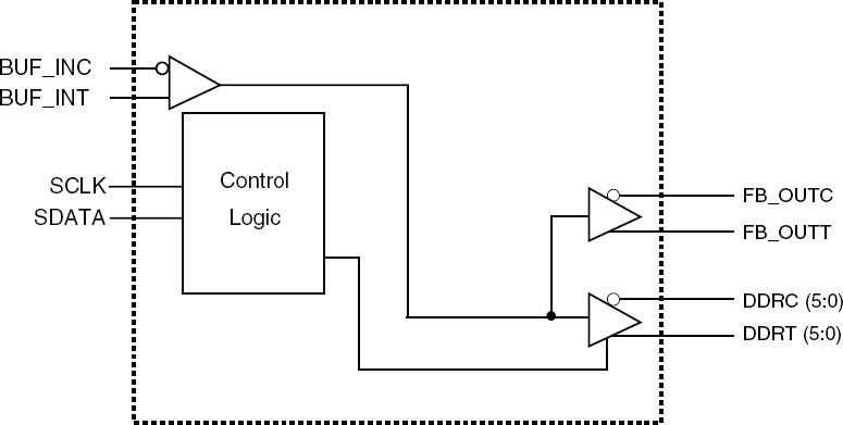
Dual DDR I/II fanout buffer for VIA Chipset
Features
- Low skew, fanout buffer
- SMBus for functional and output control
- Single bank 1-6 differential clock distribution
- 1 pair of differential feedback pins for input to output synchronization
- Supports up to 2 DDR DIMMs
- 266MHz (DDRI 533) output frequency support
- 400MHz (DDRII 800) output frequency support
- Programmable skew through SMBus
- Individual output control programmable through SMBus
- OUTPUT - OUTPUT skew: <100ps
- Output Rise and Fall Time for DDR outputs: 650ps - 950ps
- DUTY CYCLE: 47% - 53%
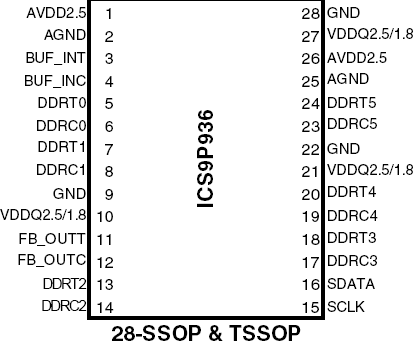
- 28-pin SSOP/TSSOP package
- RoHS compliant packaging
Comparison
Applications
Design & Development
Models
ECAD Models
Schematic symbols, PCB footprints, and 3D CAD models from SamacSys can be found by clicking on products in the Product Options table. If a symbol or model isn't available, it can be requested directly from the website.

Processing table
| SSOP | 28 | C | Yes | Tube | ||
| SSOP | 28 | C | Yes | Reel | ||
| TSSOP | 28 | C | Yes | Tube | ||
| TSSOP | 28 | C | Yes | Reel |

Tips for Using This Parametric Table:
- Hide Filters button in header: Collapse or expands filters
- Column sort buttons in header: Sort Column alphabetically / numerically descending or ascending
- Reset button in header: Reset all filters to the page default
- Full Screen button in header: Expand the table to full screen view (user must close out of full screen before they can interact with rest of page)
- Export button in header: Export the filtered results of the table to an Excel document
- Filter parts search bar in header: Type to filter table results by part number
- Hide column button in column headers: Select to hide columns in table
- AND / OR toggle switches in header: Toggles the logic of this particular filter to be “AND” or “OR” logic for filtering results
- Multiselect checkboxes at beginning of each row in table: Select these checkboxes to compare products against each other
- Document icon next to product name in row: View the featured document for this product
- Chip icon next to the right of the document icon in row: View the block diagram for this product
- Cart icon to the right of the chip icon: Indicates that samples are available for this product