Overview
Description
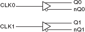
The 85222 is a Dual LVCMOS / LVTTL-to- Differential LVHSTL Translator. The 85222 has two single ended clock inputs. The single ended clock input accepts LVCMOS or LVTTL input levels and translates them to LVHSTL levels. The small outline 8-pin SOIC package makes this device ideal for applications where space, high performance and low power are important. For optimum performance, both output pairs need to be terminated, even if one output pair is unused.

Features
- 2 differential LVHSTL outputs
- Selectable CLK0, CLK1 LVCMOS clock inputs
- CLK0 and CLK1 can accept the following input levels: LVCMOS or LVTTL
- Maximum output frequency: 350MHz
- Part-to-part skew: 350ps (maximum)
- Propagation delay: 1.3ns (maximum)
- VOH: 1.2V (maximum)
- 3.3V and 2.5V operating supply
- 0°C to 70°C ambient operating temperature
- Industrial temperature information available upon request
- Lead-Free package fully RoHS compliant
Comparison
Applications
Design & Development
Models
ECAD Models
Schematic symbols, PCB footprints, and 3D CAD models from SamacSys can be found by clicking on products in the Product Options table. If a symbol or model isn't available, it can be requested directly from the website.

Processing table
| SOIC | 8 | C | Yes | Tube | ||
| SOIC | 8 | C | Yes | Reel |

Tips for Using This Parametric Table:
- Hide Filters button in header: Collapse or expands filters
- Column sort buttons in header: Sort Column alphabetically / numerically descending or ascending
- Reset button in header: Reset all filters to the page default
- Full Screen button in header: Expand the table to full screen view (user must close out of full screen before they can interact with rest of page)
- Export button in header: Export the filtered results of the table to an Excel document
- Filter parts search bar in header: Type to filter table results by part number
- Hide column button in column headers: Select to hide columns in table
- AND / OR toggle switches in header: Toggles the logic of this particular filter to be “AND” or “OR” logic for filtering results
- Multiselect checkboxes at beginning of each row in table: Select these checkboxes to compare products against each other
- Document icon next to product name in row: View the featured document for this product
- Chip icon next to the right of the document icon in row: View the block diagram for this product
- Cart icon to the right of the chip icon: Indicates that samples are available for this product