Overview
Description
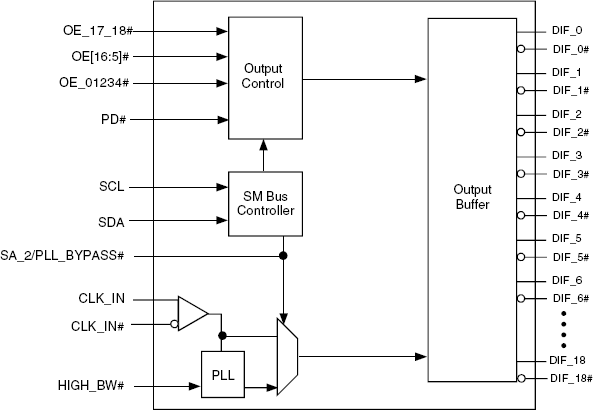
The CV145 differential buffer complies with Intel DB1900G , and is designed to work in conjunction with the main clock of CK409, CK410/CK410M and CK410B etc., PLL is off in bypass mode and no clock detect.
Features
- Compliant with Intel DB1900G
- DIF Clock Support 19 differential clock output pairs @ 0.7 V 150 ps skew performance across all outputs
- OE pin Control of All Outputs
- 3.3 V Operation
- Gear Ratio supporting generation of clocks at a different frequency ratioed from the input.
- Split outputs supporting options of 2 outputs @1:1 and remaining 17 pairs at an alternate gear
- Pin level OE control of individual outputs
- Multiple output frequency options up to 400Mhz as a gear ratio of input clocks of 100-400Mhz
- Output is HCSL compatible
- SMBus Programmable configurations
- PLL Bypass Configurable
- SMBus address configurable to allow multiple buffer control in a single control network
- Programmable Bandwidth
- Glitchfree transition between frequency states
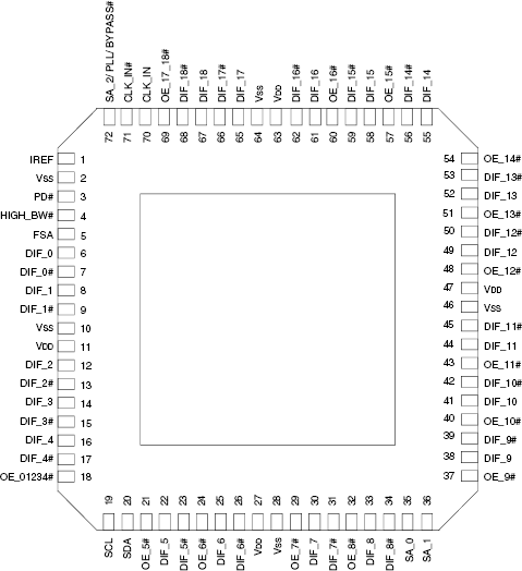
- Available in 72-pin VFQPFN package
Comparison
Applications
Design & Development
Models
ECAD Models
Schematic symbols, PCB footprints, and 3D CAD models from SamacSys can be found by clicking on products in the Product Options table. If a symbol or model isn't available, it can be requested directly from the website.

Processing table
| VFQFPN | 72 | C | Yes | Tray |

Tips for Using This Parametric Table:
- Hide Filters button in header: Collapse or expands filters
- Column sort buttons in header: Sort Column alphabetically / numerically descending or ascending
- Reset button in header: Reset all filters to the page default
- Full Screen button in header: Expand the table to full screen view (user must close out of full screen before they can interact with rest of page)
- Export button in header: Export the filtered results of the table to an Excel document
- Filter parts search bar in header: Type to filter table results by part number
- Hide column button in column headers: Select to hide columns in table
- AND / OR toggle switches in header: Toggles the logic of this particular filter to be “AND” or “OR” logic for filtering results
- Multiselect checkboxes at beginning of each row in table: Select these checkboxes to compare products against each other
- Document icon next to product name in row: View the featured document for this product
- Chip icon next to the right of the document icon in row: View the block diagram for this product
- Cart icon to the right of the chip icon: Indicates that samples are available for this product