Overview
Description
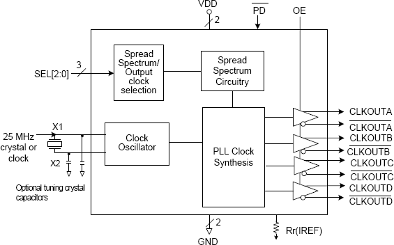
The 5V41066 is a PCIe Gen2 compliant spread-spectrum-capable clock generator. The device has 4 differential HCSL outputs and can be used in communication or embedded systems to substantially reduce electro-magnetic interference (EMI). The spread amount and output frequency are selectable via select pins.
Features
- 4 - 0.7V current mode differential HCSL output pairs
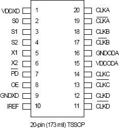
- 20-pin TSSOP package
- small board footprint
- Spread-spectrum capable
- reduces EMI
- Outputs can be terminated to LVDS
- can drive a wider variety of devices
- Power down pin
- greater system power management
- OE control pin
- greater system power management
- Spread% and frequency pin selection
- no software required to configure device
- Industrial temperature range available
- supports demanding embedded applications
- For PCIe Gen3 applications, see the 5V41236
- Cycle-to-cycle jitter < 100 ps
- Output-to-output skew < 50 ps
- PCIe Gen2 phase jitter < 3.0ps RMS
Comparison
Applications
Design & Development
Models
ECAD Models
Schematic symbols, PCB footprints, and 3D CAD models from SamacSys can be found by clicking on products in the Product Options table. If a symbol or model isn't available, it can be requested directly from the website.

| TSSOP | 20 | C | Yes | Tube | 1 | 2.532 | Get Samples, | |
| TSSOP | 20 | C | Yes | Reel | 1 | |||
| TSSOP | 20 | I | Yes | Tube | 1 | 2.013 | Get Samples, | |
| TSSOP | 20 | I | Yes | Reel | 1 |

Tips for Using This Parametric Table:
- Hide Filters button in header: Collapse or expands filters
- Column sort buttons in header: Sort Column alphabetically / numerically descending or ascending
- Reset button in header: Reset all filters to the page default
- Full Screen button in header: Expand the table to full screen view (user must close out of full screen before they can interact with rest of page)
- Export button in header: Export the filtered results of the table to an Excel document
- Filter parts search bar in header: Type to filter table results by part number
- Hide column button in column headers: Select to hide columns in table
- AND / OR toggle switches in header: Toggles the logic of this particular filter to be “AND” or “OR” logic for filtering results
- Multiselect checkboxes at beginning of each row in table: Select these checkboxes to compare products against each other
- Document icon next to product name in row: View the featured document for this product
- Chip icon next to the right of the document icon in row: View the block diagram for this product
- Cart icon to the right of the chip icon: Indicates that samples are available for this product
Videos & Training
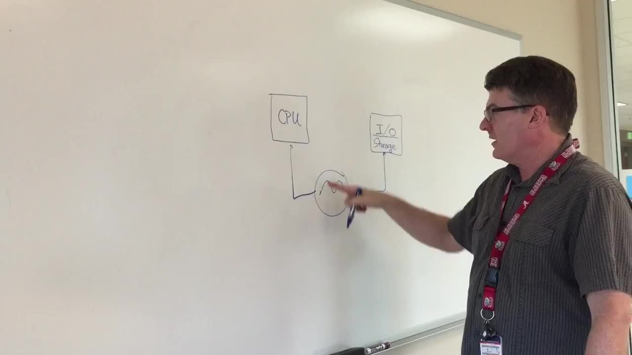
This is the first video in our PCIe series. In this video, we define PCIe architectures, focusing on common and separate clock architectures. Watch the rest of the video series below where Ron will cover the impact of different timing architectures.
Watch the Video Series Below