Overview
Description
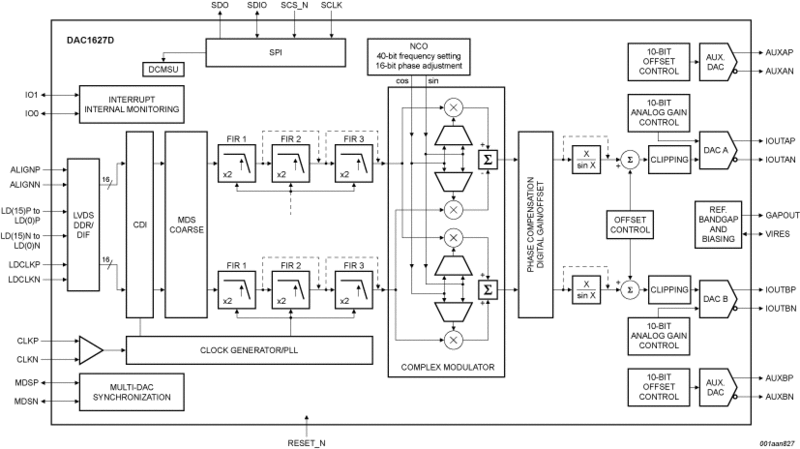
The DAC1627D1G25 is a 16-bit dual-channel digital-to-analog converter (DAC) with selectable 2x, 4x, and 8x interpolation filters optimized for multi-carrier broadband wireless transmitters at sample rates up to 1.25Gsps. Supplied from 3.3V and 1.8V power sources, it integrates a differential scalable output current up to 34mA. The mixer frequency is set by a high-resolution 40-bit numerically controlled oscillator (NCO). High-resolution internal gain, phase, and offset control provide outstanding image and LO rejection at the system analog modulator output. An inverse (sin x)/x function ensures controlled flatness at the DAC output. The LVDS DDR receiver interface allows a high data bandwidth (312.5MS/sec) at the input.
Features
- 1.25Gsps maximum update rate
- 1.8V and 3.3V power supplies
- 3-wire or 4-wire mode SPI interface
- Differential scalable output current from 8.1mA to 34mA
- Dual-channel 16-bit resolution
- Embedded complex digital modulator
- Embedded numerically controlled oscillator with 40-bit programmable frequency
- External analog offset control (10-bit auxiliary DACs)
- High-resolution internal digital gain and offset control
- Interleaved or folded I and Q data input modes
- Internal phase correction
- Inverse (sin x)/x function
- LVDS DDR compatible input interface with on-chip 100Ω termination
- LVDS DDR input clock up to 312.5MHz
- LVDS or LVPECL-compatible DAC clock
- On-chip 1.25V reference
- Power-down mode and sleep mode
- Selectable 2x, 4x, and 8x interpolation filters
- Very-low noise capacitor-free integrated Phase-Locked Loop (PLL)
Comparison
Applications
Applications
- Wireless infrastructure: MC_GSM, LTE, WiMAX, GSM, CDMA, WCDMA, TD-SCDMA
- Communications: LMDS/MMDS, point-to-point
- Direct Digital Synthesis (DDS)
- Digital radio links
- Instrumentation
- Automated Test Equipment (ATE)
Documentation
|
|
|
|
|---|---|---|
| Type | Title | Date |
| Datasheet | PDF 1014 KB | |
1 item
|
||
Design & Development
Models
ECAD Models
Schematic symbols, PCB footprints, and 3D CAD models from SamacSys can be found by clicking on products in the Product Options table. If a symbol or model isn't available, it can be requested directly from the website.

| VFQFPN | 72 | I | Yes | Tray | ||
| VFQFPN | 72 | I | Yes | Reel |

Tips for Using This Parametric Table:
- Hide Filters button in header: Collapse or expands filters
- Column sort buttons in header: Sort Column alphabetically / numerically descending or ascending
- Reset button in header: Reset all filters to the page default
- Full Screen button in header: Expand the table to full screen view (user must close out of full screen before they can interact with rest of page)
- Export button in header: Export the filtered results of the table to an Excel document
- Filter parts search bar in header: Type to filter table results by part number
- Hide column button in column headers: Select to hide columns in table
- AND / OR toggle switches in header: Toggles the logic of this particular filter to be “AND” or “OR” logic for filtering results
- Multiselect checkboxes at beginning of each row in table: Select these checkboxes to compare products against each other
- Document icon next to product name in row: View the featured document for this product
- Chip icon next to the right of the document icon in row: View the block diagram for this product
- Cart icon to the right of the chip icon: Indicates that samples are available for this product