Overview
Description
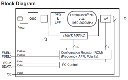
The 8N0Q001 is a quad-frequency programmable clock oscillator with very flexible frequency programming capabilities. The device uses Renesas' fourth-generation FemtoClock®NG technology for an optimum of high clock frequency and low phase noise performance. The device accepts 2.5V or 3.3V supply and is packaged in a small, lead-free (RoHS 6) 10-lead ceramic 5mm x 7mm x 1.55mm package.
Besides the four default power-up frequencies set by the FSEL0 and FSEL1 pins, the 8N0Q001 can be programmed via the I2C interface to output clock frequencies between 15.476MHz and 260MHz to a very high degree of precision with a frequency step size of 435.9Hz ÷ N (N: PLL post divider). Since the FSEL0 and FSEL1 pins are mapped to four independent PLL M and N divider registers (P, MINT, MFRAC, and N), reprogramming those registers to other frequencies under control of FSEL0 and FSEL1 is supported. The extended temperature range supports wireless infrastructure, telecommunication, and networking end equipment requirements.
Features
- Fourth generation FemtoClock® NG technology
- Programmable clock output frequency from 15.476MHz to 260MHz
- Four power-up default frequencies (see part number order codes), re-programmable by I2C
- I2C programming interface for the output clock frequency and internal PLL control registers
- Frequency programming resolution is 435.9Hz ÷ N
- One 2.5V, 3.3V LVCMOS clock output
- Two control inputs for the power-up default frequency
- LVCMOS/LVTTL compatible control inputs
- RMS phase jitter at 156.25MHz (12kHz to 20MHz): 0.250ps (typical)
- RMS phase jitter at 156.25MHz (1kHz to 40MHz): 0.290ps (typical)
- 2.5V or 3.3V supply
- -40 °C to 85 °C ambient operating temperature
- Available in a lead-free (RoHS 6) package
Comparison
Applications
Documentation
|
|
|
|
|---|---|---|
| Type | Title | Date |
| Datasheet | PDF 707 KB | |
| Overview | PDF 526 KB | |
| Manual - Hardware | PDF 182 KB | |
| Product Brief | PDF 6.57 MB | |
| Manual - Development Tools | PDF 693 KB | |
5 items
|
||
Design & Development
Models
ECAD Models
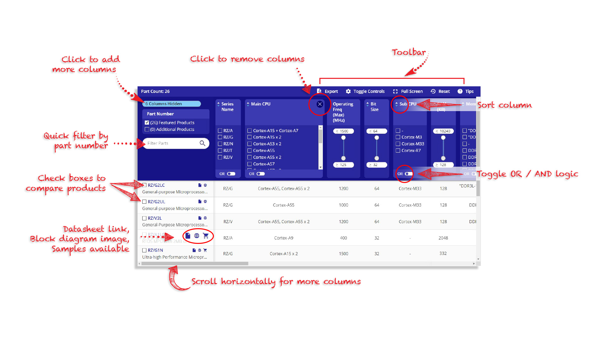
Schematic symbols, PCB footprints, and 3D CAD models from SamacSys can be found by clicking on products in the Product Options table. If a symbol or model isn't available, it can be requested directly from the website.


