Overview
Description
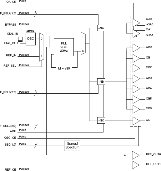
The 844S012I-01 is an optimized PCIe, sRIO and Gigabit Ethernet Frequency Synthesizer. The 844S012I-01 uses a 25MHz parallel resonant crystal to generate 33.33MHz - 200MHz clock signals, replacing solutions requiring multiple oscillator and fanout buffer solution. The device supports ±0.25% center-spread, and -0.6% down-spread clocking with two spread select pins (SSC[1:0]). The VCO operates at frequency of 2GHz. The device has three output banks: Bank A with two LVDS outputs, 100MHz – 250MHz; Bank B with seven 33.33MHz – 200MHz LVCMOS/ LVTTL outputs; and Bank C with one 33.33MHz – 200MHz LVCMOS/LVTTL output.
All Banks A, B and C have their own dedicated frequency select pins and can be independently set for the frequencies mentioned above. The low jitter characteristic of the 844S012I-01 makes it an ideal clock source for PCIe, sRIO and Gigabit Ethernet applications. Designed for networking and industrial applications, the 844S012I-01 can also drive the high-speed clock inputs of communication processors, DSPs, switches and bridges. The 843241I-04 is a Serial ATA (SATA)/Serial Attached SCSI (SAS) Clock Generator and a member of the HiPerClocksTM family of high performance devices from IDT. For SATA/SAS applications, a 25MHz crystal is used to produce 150MHz. The 843241I-04 is packaged in a small 8-pin TSSOP, making it ideal for use in systems with limited board space.
Features
- Two differential LVDS outputs (Bank A), configurable for PCIe (100MHz or 250MHz) and sRIO (100MHz or 125MHz) clock signals
- Eight LVCMOS/LVTTL outputs (Bank B/C), 18Ω typical output impedance
- Two REF_OUT LVCMOS/LVTTL clock outputs 23Ω typical output impedance
- Selectable crystal oscillator interface, 25MHz, 18pF parallel resonant crystal or one LVCMOS/LVTTL single-ended reference clock input
- Supports the following output frequencies: LVDS Bank A: 100MHz, 125MHz, 200MHz and 250MHz LVCMOS/LVTTL Bank B/C: 33.33MHz, 50MHz, 66.67MHz, 100MHz, 125MHz, 133.33MHz, 166.67MHz and 200MHz
- VCO: 2GHz
- Spread spectrum clock: ±0.25% center-spread, and -0.6% down-spread
- PLL bypass and output enable
- RMS period jitter: 23ps (maximum), QB outputs
- Full 3.3V supply voltage
- -40°C to 85°C ambient operating temperature
- Available in a lead-free (RoHS 6) compliant package
Comparison
Applications
Design & Development
Models
ECAD Models
Schematic symbols, PCB footprints, and 3D CAD models from SamacSys can be found by clicking on products in the Product Options table. If a symbol or model isn't available, it can be requested directly from the website.

| VFQFPN | 56 | I | Yes | Tray | ||
| VFQFPN | 56 | I | Yes | Reel |

Tips for Using This Parametric Table:
- Hide Filters button in header: Collapse or expands filters
- Column sort buttons in header: Sort Column alphabetically / numerically descending or ascending
- Reset button in header: Reset all filters to the page default
- Full Screen button in header: Expand the table to full screen view (user must close out of full screen before they can interact with rest of page)
- Export button in header: Export the filtered results of the table to an Excel document
- Filter parts search bar in header: Type to filter table results by part number
- Hide column button in column headers: Select to hide columns in table
- AND / OR toggle switches in header: Toggles the logic of this particular filter to be “AND” or “OR” logic for filtering results
- Multiselect checkboxes at beginning of each row in table: Select these checkboxes to compare products against each other
- Document icon next to product name in row: View the featured document for this product
- Chip icon next to the right of the document icon in row: View the block diagram for this product
- Cart icon to the right of the chip icon: Indicates that samples are available for this product