Overview
Description
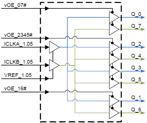
The 9SBV0802 provides two banks of four 1.05V LVCMOS outputs. Each bank has its own input. There are three OE pins. Two OE pins control two outputs each and one OE pin controls four outputs. One 9SBV0802 allows one PCH to easily support four CPUs with point-to-point routing of the PM signals. Two 9SBV0802 devices allow one PCH to easily support up to eight CPUs with point-to-point routing of the PM signals.
Features
- Eight 1MHz – 48MHz 1.05V LVCMOS outputs
- Additive cycle-to-cycle jitter < 8ps
- Output-to-output skew within a bank < 50ps
- Output-to-output skew between banks < 100ps
- 1.8V power supply, 15mW typical power consumption
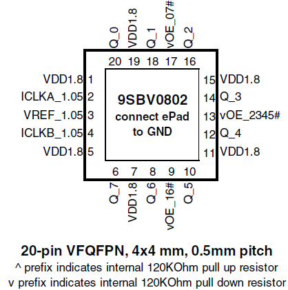
- Three OE pins
- 1.05V LVCMOS inputs with VREF pin
- Space saving 4mm x 4mm 20-VFQFPN
Comparison
Applications
Applications
- Fanout buffer for PM-SYNC and PM_SYNC CLK in Intel servers
Design & Development
Models
ECAD Models
Schematic symbols, PCB footprints, and 3D CAD models from SamacSys can be found by clicking on products in the Product Options table. If a symbol or model isn't available, it can be requested directly from the website.

| VFQFPN | 20 | I | -40 to 85°C | Tray | 1 | 6.162 | Get Samples, | |
| VFQFPN | 20 | I | -40 to 85°C | Reel | 1 | 6.862 |

Tips for Using This Parametric Table:
- Hide Filters button in header: Collapse or expands filters
- Column sort buttons in header: Sort Column alphabetically / numerically descending or ascending
- Reset button in header: Reset all filters to the page default
- Full Screen button in header: Expand the table to full screen view (user must close out of full screen before they can interact with rest of page)
- Export button in header: Export the filtered results of the table to an Excel document
- Filter parts search bar in header: Type to filter table results by part number
- Hide column button in column headers: Select to hide columns in table
- AND / OR toggle switches in header: Toggles the logic of this particular filter to be “AND” or “OR” logic for filtering results
- Multiselect checkboxes at beginning of each row in table: Select these checkboxes to compare products against each other
- Document icon next to product name in row: View the featured document for this product
- Chip icon next to the right of the document icon in row: View the block diagram for this product
- Cart icon to the right of the chip icon: Indicates that samples are available for this product
Videos & Training
This video overviews the LVCMOS Fanout Buffers, showcasing their best-in-class performance with extremely low phase jitter, minimal output skew, and low power consumption, along with other competitive features.
News & Blog Posts
| News | Mar 24, 2015 |
