Overview
Description
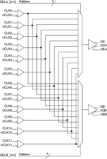
The 854S202I is a 12:2 Differential-to-LVDS Clock Multiplexer which can operate >3GHz. The 854S202I has 12 selectable differential clock inputs, any of which can be independently routed to either of the two LVDS outputs. The CLKx, nCLKx input pairs can accept LVPECL, LVDS, CML or SSTL levels. The fully differential architecture and low propagation delay make it ideal for use in clock distribution circuits.
Features
- Two differential 3.3V LVDS clock outputs
- Twelve selectable differential clock inputs
- CLKx, nCLKx pairs can accept the following differential input levels: LVPECL, LVDS, HSTL, SSTL, HCSL
- Maximum output frequency: >3GHz
- Propagation delay: 660ps (typical)
- Input skew: TBD
- Output skew: 25ps (typical)
- Part-to-part skew: TBD
- Additive phase jitter, RMS: 0.16ps (typical)
- Full 3.3V operating supply mode
- -40°C to 85°C ambient operating temperature
- Available in lead-free (RoHS 6) package
Comparison
Applications
Design & Development
Models
ECAD Models
Schematic symbols, PCB footprints, and 3D CAD models from SamacSys can be found by clicking on products in the Product Options table. If a symbol or model isn't available, it can be requested directly from the website.

Processing table
| TQFP | 48 | I | Yes | Tray | ||
| TQFP | 48 | I | Yes | Reel |

Tips for Using This Parametric Table:
- Hide Filters button in header: Collapse or expands filters
- Column sort buttons in header: Sort Column alphabetically / numerically descending or ascending
- Reset button in header: Reset all filters to the page default
- Full Screen button in header: Expand the table to full screen view (user must close out of full screen before they can interact with rest of page)
- Export button in header: Export the filtered results of the table to an Excel document
- Filter parts search bar in header: Type to filter table results by part number
- Hide column button in column headers: Select to hide columns in table
- AND / OR toggle switches in header: Toggles the logic of this particular filter to be “AND” or “OR” logic for filtering results
- Multiselect checkboxes at beginning of each row in table: Select these checkboxes to compare products against each other
- Document icon next to product name in row: View the featured document for this product
- Chip icon next to the right of the document icon in row: View the block diagram for this product
- Cart icon to the right of the chip icon: Indicates that samples are available for this product