Overview
Description
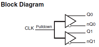
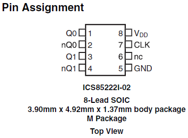
The ICS85222I-02 is a 1-to-2 LVCMOS/LVTTL-to-differential HSTL translator. The ICS85222I-02 has one single-ended clock input. The single-ended clock input accepts LVCMOS or LVTTL input levels and translates them to HSTL levels. The small outline 8-pin SOIC package makes this device ideal for applications where space, high performance, and low power are important.
Features
- Two differential HSTL outputs
- One LVCMOS/LVTTL clock input
- CLK input can accept the following input levels: LVCMOS or LVTTL
- Maximum output frequency: 350MHz
- Part-to-Part skew: 500ps (maximum)
- Propagation delay: 1.55ns (maximum)
- VOH: 1.4V (maximum)
- Output crossover voltage: 0.5V to 0.9V
- Full 3.3V operating supply voltage
- -40 °C to 85 °C ambient operating temperature
- Lead-free RoHS compliant packaging
Comparison
Applications
Design & Development
Models
ECAD Models
Schematic symbols, PCB footprints, and 3D CAD models from SamacSys can be found by clicking on products in the Product Options table. If a symbol or model isn't available, it can be requested directly from the website.


