Overview
Description
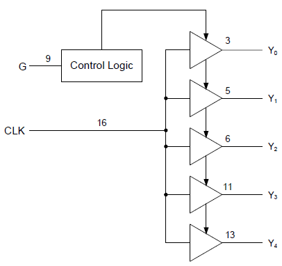
The IDT5V2305 is a high performance, low skew clock buffer that operates up to 200MHz. One bank of five outputs provides low skew copies of CLK. Through the use of control pin G, the outputs of bank Y(0:4) can be placed in a low state regardless of CLK input. The device operates in 2.5V and 3.3V environments. The built-in output enable glitch suppression ensures a synchronized output enable sequence to distribute full period clock signals. The IDT5V2305 is characterized for operation from -40°C to +85°C.
Features
- High performance 1:5 clock driver for general purpose applications
- Operates up to 170MHz at VDD = 2.5V
- Operates up to 200MHz at VDD = 3.3V
- Pin-to-pin skew < 75ps at 3.3V operation
- VDD range: 2.3V to 3.6V
- Output enable glitch suppression
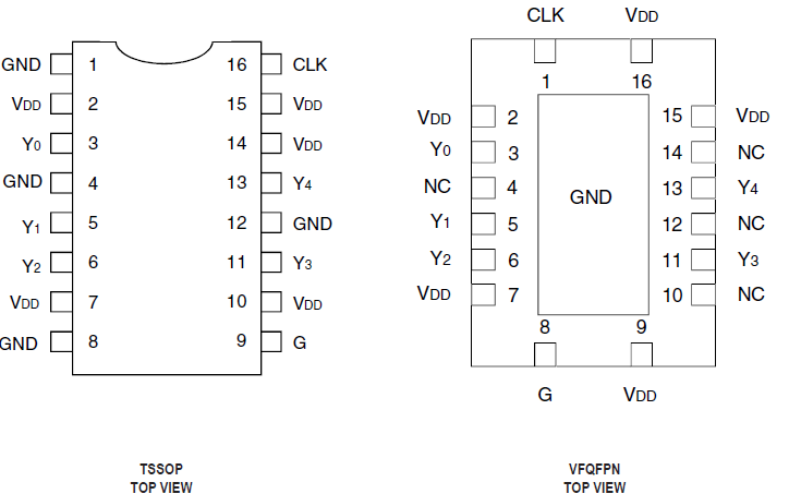
- Available in TSSOP and VFQFPN packages
Comparison
Applications
Design & Development
Models
ECAD Models
Schematic symbols, PCB footprints, and 3D CAD models from SamacSys can be found by clicking on products in the Product Options table. If a symbol or model isn't available, it can be requested directly from the website.

Processing table
| VFQFPN | 16 | I | Yes | Cut Tape | 2.022 | ||
| VFQFPN | 16 | I | Yes | Reel | 2.022 | ||
| TSSOP | 16 | I | Yes | Tube | 1.887 | ||
| TSSOP | 16 | I | Yes | Reel | 2.135 |

Tips for Using This Parametric Table:
- Hide Filters button in header: Collapse or expands filters
- Column sort buttons in header: Sort Column alphabetically / numerically descending or ascending
- Reset button in header: Reset all filters to the page default
- Full Screen button in header: Expand the table to full screen view (user must close out of full screen before they can interact with rest of page)
- Export button in header: Export the filtered results of the table to an Excel document
- Filter parts search bar in header: Type to filter table results by part number
- Hide column button in column headers: Select to hide columns in table
- AND / OR toggle switches in header: Toggles the logic of this particular filter to be “AND” or “OR” logic for filtering results
- Multiselect checkboxes at beginning of each row in table: Select these checkboxes to compare products against each other
- Document icon next to product name in row: View the featured document for this product
- Chip icon next to the right of the document icon in row: View the block diagram for this product
- Cart icon to the right of the chip icon: Indicates that samples are available for this product