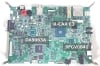
R-Car V4H System Evaluation Board Set/White Hawk
The White Hawk is an R-Car V4H-specific evaluation board set that can be used to evaluate systems using the R-Car V4H and to develop operating systems, device drivers,...

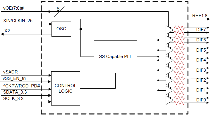
The 9FGV0841 is an 8-output very low power clock generator for PCIe Gen1–4 applications with integrated output terminations providing Zo=100 Ω. The device has 8 output enables for clock management and supports 2 different spread spectrum levels in addition to spread off.
For information regarding evaluation boards and material, please contact your local IDT sales representative.
The White Hawk is an R-Car V4H-specific evaluation board set that can be used to evaluate systems using the R-Car V4H and to develop operating systems, device drivers,...
The combination of R-Car E3 and Clock Generator provides the optimized function and performance for full graphic cluster solutions, supporting large panels of an...
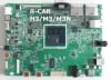
The combination of R-Car (H3/M3/M3N) SiP and the Clock Generators provides high efficiency and supports a variety of display outputs and high-quality outputs for...
Schematic symbols, PCB footprints, and 3D CAD models from SamacSys can be found by clicking on products in the Product Options table. If a symbol or model isn't available, it can be requested directly from the website.

| VFQFPN | 48 | I | Yes | Tray | 3 | 2.347 | Get Samples, | |
| VFQFPN | 48 | I | Yes | Reel | 3 | |||
| VFQFPN | 48 | C | Yes | Tray | 3 | 2.149 | Get Samples, | |
| VFQFPN | 48 | C | Yes | Reel | 3 | |||
| VFQFPN | 48 | 2 | Yes | Tray | 3 | Get Samples, | ||
| VFQFPN | 48 | 2 | Yes | Reel | 3 |

IDT’s chief PCIe system architect explains the fundamental difference in reference clock jitter budgets between the first three generations of the specification and those of Gen4 and Gen5 which raise new challenges for designers.
| Blog Post | Apr 14, 2022 | ||
| Blog Post | Feb 7, 2019 | ||
| Blog Post | May 22, 2018 | ||
| News | Apr 30, 2018 |