概要
説明
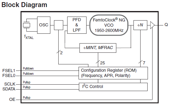
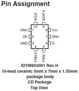
The 8N0Q001 is a quad-frequency programmable clock oscillator with very flexible frequency programming capabilities. The device uses Renesas' fourth-generation FemtoClock®NG technology for an optimum of high clock frequency and low phase noise performance. The device accepts 2.5V or 3.3V supply and is packaged in a small, lead-free (RoHS 6) 10-lead ceramic 5mm x 7mm x 1.55mm package.
Besides the four default power-up frequencies set by the FSEL0 and FSEL1 pins, the 8N0Q001 can be programmed via the I2C interface to output clock frequencies between 15.476MHz and 260MHz to a very high degree of precision with a frequency step size of 435.9Hz ÷ N (N: PLL post divider). Since the FSEL0 and FSEL1 pins are mapped to four independent PLL M and N divider registers (P, MINT, MFRAC, and N), reprogramming those registers to other frequencies under control of FSEL0 and FSEL1 is supported. The extended temperature range supports wireless infrastructure, telecommunication, and networking end equipment requirements.
特長
- Fourth generation FemtoClock® NG technology
- Programmable clock output frequency from 15.476MHz to 260MHz
- Four power-up default frequencies (see part number order codes), re-programmable by I2C
- I2C programming interface for the output clock frequency and internal PLL control registers
- Frequency programming resolution is 435.9Hz ÷ N
- One 2.5V, 3.3V LVCMOS clock output
- Two control inputs for the power-up default frequency
- LVCMOS/LVTTL compatible control inputs
- RMS phase jitter at 156.25MHz (12kHz to 20MHz): 0.250ps (typical)
- RMS phase jitter at 156.25MHz (1kHz to 40MHz): 0.290ps (typical)
- 2.5V or 3.3V supply
- -40 °C to 85 °C ambient operating temperature
- Available in a lead-free (RoHS 6) package
製品比較
アプリケーション
ドキュメント
|
|
|
|
|---|---|---|
| 分類 | タイトル | 日時 |
| データシート | PDF 707 KB | |
| 概要 | PDF 526 KB | |
| マニュアル-ハードウェア | PDF 182 KB | |
| 製品概要 | PDF 6.57 MB | |
| マニュアル-開発ツール | PDF 693 KB | |
5 items
|
||
設計・開発
モデル
ECADモデル
[製品選択]テーブル内の製品名をクリックするとSamacSysが提供する回路図シンボル、PCBフットプリント、3D CADモデルがご確認いただけます。 お探しのシンボルやモデルが見つからない場合、Webサイトから直接リクエストできます。

| CLCC | 10 | I | Yes | Tray | 1 | サンプルを入手, |

Tips for Using This Parametric Table:
- Hide Filters button in header: Collapse or expands filters
- Column sort buttons in header: Sort Column alphabetically / numerically descending or ascending
- Reset button in header: Reset all filters to the page default
- Full Screen button in header: Expand the table to full screen view (user must close out of full screen before they can interact with rest of page)
- Export button in header: Export the filtered results of the table to an Excel document
- Filter parts search bar in header: Type to filter table results by part number
- Hide column button in column headers: Select to hide columns in table
- AND / OR toggle switches in header: Toggles the logic of this particular filter to be “AND” or “OR” logic for filtering results
- Multiselect checkboxes at beginning of each row in table: Select these checkboxes to compare products against each other
- Document icon next to product name in row: View the featured document for this product
- Chip icon next to the right of the document icon in row: View the block diagram for this product
- Cart icon to the right of the chip icon: Indicates that samples are available for this product