概要
説明
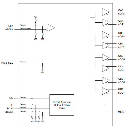
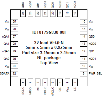
The IDT8T79S838-08I is a high performance, 1-to-8, differential input to universal output fanout buffer. The device is designed for signal fanout of high-frequency clock signals in applications requiring output frequencies generated simultaneously. The IDT8T79S838-08I is optimized for 3.3V and 2.5V supply voltages and a temperature range of -40°C to 85°C. The device is packaged in a space-saving 32 lead VFQFN package.
特長
- Four banks of two output pairs
- Individual output type control, LVDS or LVPECL, via serial interface
- Individual outputs remain enabled while serial loading new device configurations
- One differential PCLK, nPCLK input
- PCLK, nPCLK input pair can accept the following differential input levels: LVPECL, LVDS levels
- Maximum input frequency: 1.5GHz
- LVCMOS control inputs
- Individual output enable/disable control via serial interface
- 2.375V to 3.465V supply voltage operation
- -40°C to 85°C ambient operating temperature
- Lead-free (RoHS 6) packaging
製品比較
アプリケーション
設計・開発
モデル
ECADモデル
[製品選択]テーブル内の製品名をクリックするとSamacSysが提供する回路図シンボル、PCBフットプリント、3D CADモデルがご確認いただけます。 お探しのシンボルやモデルが見つからない場合、Webサイトから直接リクエストできます。

Processing table
| VFQFPN | 32 | I | Yes | Tray | ||
| VFQFPN | 32 | I | Yes | Reel |

Tips for Using This Parametric Table:
- Hide Filters button in header: Collapse or expands filters
- Column sort buttons in header: Sort Column alphabetically / numerically descending or ascending
- Reset button in header: Reset all filters to the page default
- Full Screen button in header: Expand the table to full screen view (user must close out of full screen before they can interact with rest of page)
- Export button in header: Export the filtered results of the table to an Excel document
- Filter parts search bar in header: Type to filter table results by part number
- Hide column button in column headers: Select to hide columns in table
- AND / OR toggle switches in header: Toggles the logic of this particular filter to be “AND” or “OR” logic for filtering results
- Multiselect checkboxes at beginning of each row in table: Select these checkboxes to compare products against each other
- Document icon next to product name in row: View the featured document for this product
- Chip icon next to the right of the document icon in row: View the block diagram for this product
- Cart icon to the right of the chip icon: Indicates that samples are available for this product