概要
説明
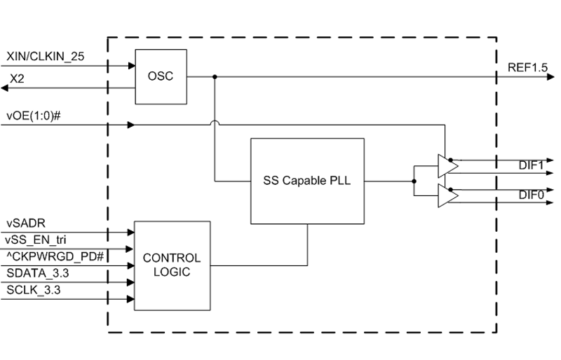
The 9FGU0231 is a member of IDT's 1.5 V Ultra-Low-Power PCIe clock family. The device has 2 output enables for clock management, 2 different spread spectrum levels in addition to spread off, and 2 selectable SMBus addresses.
特長
-
LP-HCSL outputs; save 4 resistors compared to standard PCIe devices
-
23 mW typical power consumption; reduced thermal concerns
-
OE# pins; support DIF power management
-
Programmable slew rate for each output; allows tuning for various line lengths
-
Programmable output amplitude; allows tuning for various application environments
-
DIF outputs blocked until PLL is locked; clean system start-up
-
Selectable 0%, -0.25% or -0.5% spread on DIF outputs; reduces EMI
-
External 25 MHz crystal; supports tight ppm with 0 ppm synthesis error
-
Configuration can be accomplished with strapping pins; SMBus interface not required for device control
-
3.3 V tolerant SMBus interface works with legacy controllers
-
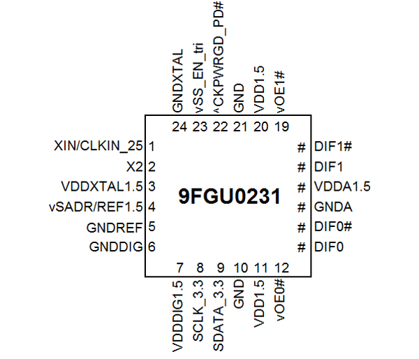
Space saving 4x4 mm 24-pin VFQFPN; minimal board space
-
Selectable SMBus addresses; multiple devices can easily share an SMBus segment
製品比較
アプリケーション
設計・開発
モデル
ECADモデル
[製品選択]テーブル内の製品名をクリックするとSamacSysが提供する回路図シンボル、PCBフットプリント、3D CADモデルがご確認いただけます。 お探しのシンボルやモデルが見つからない場合、Webサイトから直接リクエストできます。

Processing table

Tips for Using This Parametric Table:
- Hide Filters button in header: Collapse or expands filters
- Column sort buttons in header: Sort Column alphabetically / numerically descending or ascending
- Reset button in header: Reset all filters to the page default
- Full Screen button in header: Expand the table to full screen view (user must close out of full screen before they can interact with rest of page)
- Export button in header: Export the filtered results of the table to an Excel document
- Filter parts search bar in header: Type to filter table results by part number
- Hide column button in column headers: Select to hide columns in table
- AND / OR toggle switches in header: Toggles the logic of this particular filter to be “AND” or “OR” logic for filtering results
- Multiselect checkboxes at beginning of each row in table: Select these checkboxes to compare products against each other
- Document icon next to product name in row: View the featured document for this product
- Chip icon next to the right of the document icon in row: View the block diagram for this product
- Cart icon to the right of the chip icon: Indicates that samples are available for this product
ビデオ&トレーニング
PCIe Clocking Architectures (Common and Separate)
This is the first video in our PCIe series. In this video, we define PCIe architectures, focusing on common and separate clock architectures. Watch the rest of the video series below where Ron will cover the impact of different timing architectures.
Watch the Video Series Below
Video List
ニュース&ブログ
| ブログ | 2022年4月14日 | ||
| ブログ | 2018年5月22日 | ||
| ニュース | 2018年4月30日 |


