概要
説明
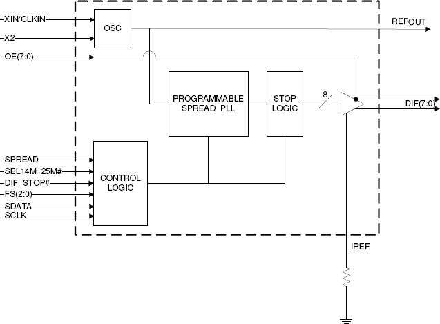
The 9FG830 is a Frequency Timing Generator that provides 8 HCSL differential output pairs. These outputs support PCI-Express Gen3, and QPI applications. The part supports Spread Spectrum and synthesizes several additional output frequencies from either a 14.31818 MHz crystal, a 25 MHz crystal or reference input clock. The 9FG830 also outputs a copy of the reference clock. Complete control of the device is available via strapping pins or via the SMBus interface.
特長
- 8 - 0.7 V current mode differential HCSL output pairs
- 1 - 3.3 V LVTTL REF output
- Pin-to-Pin with 9FG108D
- Easy upgrade to PCIe Gen3
- Generates common frequencies from 14.318 MHz or 25 MHz; single part supports multiple applications
- Provides copy of reference output; eliminates need for additional crystal or oscillator
- Three spread spectrum modes: -0.5%, +/-0.25%, and off; EMI reduction
- Unused outputs may be disabled in Hi-Z; save system power
- Device may be configured by SMBus and/or strap pins; can be used in systems without SMBus
- Cycle-to-cycle jitter: < 50 ps with 25 MHz input
- Output-to-output skew: <50 ps
- Phase jitter: PCIe Gen3 < 1 ps RMS
- Phase jitter: QPI 9.6GB/s < 0.2 ps RMS
- 10 ppm synthesis error with 25 MHz input and Spread Off
製品比較
アプリケーション
設計・開発
モデル
ECADモデル
[製品選択]テーブル内の製品名をクリックするとSamacSysが提供する回路図シンボル、PCBフットプリント、3D CADモデルがご確認いただけます。 お探しのシンボルやモデルが見つからない場合、Webサイトから直接リクエストできます。

| SSOP | 48 | I | Yes | Tube | ||
| SSOP | 48 | I | Yes | Reel | ||
| SSOP | 48 | C | Yes | Tube | ||
| SSOP | 48 | C | Yes | Reel | ||
| TSSOP | 48 | I | Yes | Tube | ||
| TSSOP | 48 | I | Yes | Reel | ||
| TSSOP | 48 | C | Yes | Tube | ||
| TSSOP | 48 | C | Yes | Reel |

Tips for Using This Parametric Table:
- Hide Filters button in header: Collapse or expands filters
- Column sort buttons in header: Sort Column alphabetically / numerically descending or ascending
- Reset button in header: Reset all filters to the page default
- Full Screen button in header: Expand the table to full screen view (user must close out of full screen before they can interact with rest of page)
- Export button in header: Export the filtered results of the table to an Excel document
- Filter parts search bar in header: Type to filter table results by part number
- Hide column button in column headers: Select to hide columns in table
- AND / OR toggle switches in header: Toggles the logic of this particular filter to be “AND” or “OR” logic for filtering results
- Multiselect checkboxes at beginning of each row in table: Select these checkboxes to compare products against each other
- Document icon next to product name in row: View the featured document for this product
- Chip icon next to the right of the document icon in row: View the block diagram for this product
- Cart icon to the right of the chip icon: Indicates that samples are available for this product
ビデオ&トレーニング
This is the first video in our PCIe series. In this video, we define PCIe architectures, focusing on common and separate clock architectures. Watch the rest of the video series below where Ron will cover the impact of different timing architectures.
Watch the Video Series Below