概要
説明
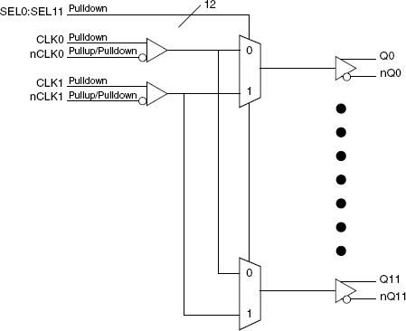
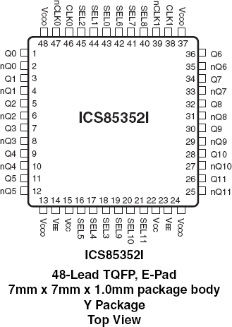
The 85352I is a 12 bit, 2-to-1 LVPECL Clock Buffer. Individual input select controls support independent multiplexer operation from a common clock input source. Clock inputs accept most standard differential levels. The 85352I is characterized at full 3.3V or mixed 3.3V core/2.5V output operating supply modes.
特長
- Twelve, 2-to-1 multiplexers with LVPECL outputs
- Selectable differential CLKx, nCLKx input pairs
- CLK, nCLK pair can accept the following differential input levels: LVPECL, LVDS, LVHSTL, HCSL, SSTL
- Maximum output frequency: 700MHz
- Individual select control for each multiplexer
- Select inputs accept LVCMOS / LVTTL levels
- Propagation delay: 2ns (maximum)
- Additive Phase Jitter, RMS: 0.21ps (typical), 3.3V
- Full 3.3V or mixed 3.3V core/2.5V output supply
- -40°C to 85°C ambient operating temperature
- Available in lead-free (RoHS 6) package
製品比較
アプリケーション
設計・開発
モデル
ECADモデル
[製品選択]テーブル内の製品名をクリックするとSamacSysが提供する回路図シンボル、PCBフットプリント、3D CADモデルがご確認いただけます。 お探しのシンボルやモデルが見つからない場合、Webサイトから直接リクエストできます。

Processing table
| PTQFP | 48 | I | Yes | Tray | ||
| PTQFP | 48 | I | Yes | Reel |

Tips for Using This Parametric Table:
- Hide Filters button in header: Collapse or expands filters
- Column sort buttons in header: Sort Column alphabetically / numerically descending or ascending
- Reset button in header: Reset all filters to the page default
- Full Screen button in header: Expand the table to full screen view (user must close out of full screen before they can interact with rest of page)
- Export button in header: Export the filtered results of the table to an Excel document
- Filter parts search bar in header: Type to filter table results by part number
- Hide column button in column headers: Select to hide columns in table
- AND / OR toggle switches in header: Toggles the logic of this particular filter to be “AND” or “OR” logic for filtering results
- Multiselect checkboxes at beginning of each row in table: Select these checkboxes to compare products against each other
- Document icon next to product name in row: View the featured document for this product
- Chip icon next to the right of the document icon in row: View the block diagram for this product
- Cart icon to the right of the chip icon: Indicates that samples are available for this product