概要
説明
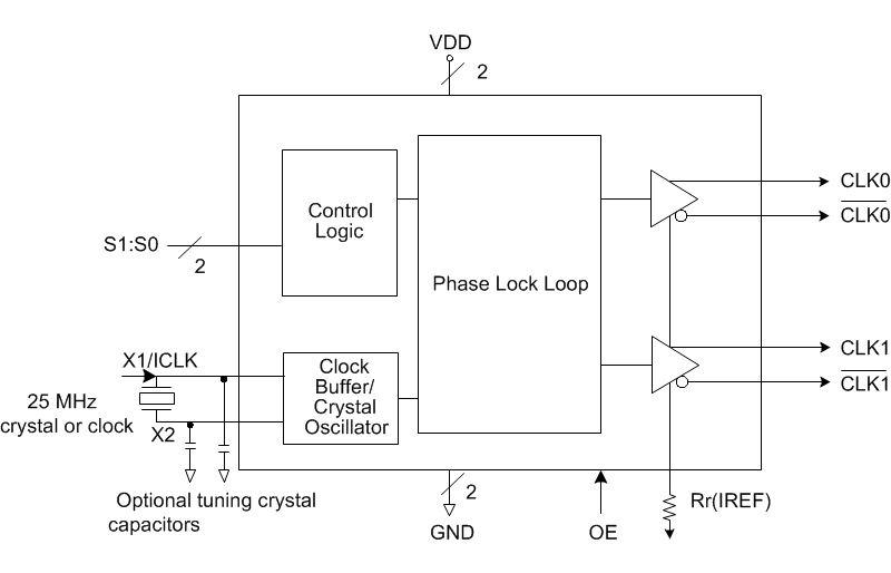
The IDT5V41285 is a PCIe Gen2 compliant clock generator. The device has 2 differential HCSL outputs. The output frequency is selectable via select pins.
特長
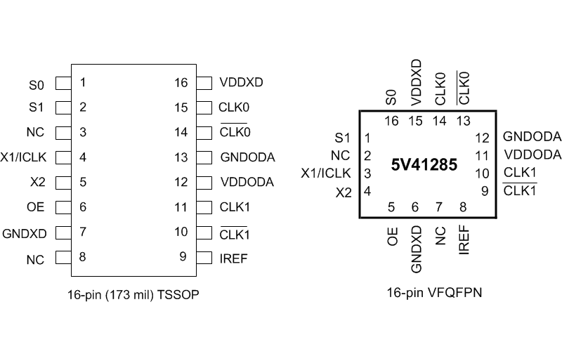
- 16-pin TSSOP and VFQFPN packages; small board footprint
- Outputs can be terminated to LVDS; can drive a wider variety of devices
- OE control pin; greater system power management
- Industrial temperature range available; supports demanding embedded applications
- Cycle-to-cycle jitter: 80ps
- Output-to-output skew <50 ps
- PCIe Gen2 phase jitter <3.0ps RMS
- Low phase noise: 12kHz to 20MHz <6ps
- For PCIe Gen3 applications, see the IDT5V41315
製品比較
アプリケーション
設計・開発
モデル
ECADモデル
[製品選択]テーブル内の製品名をクリックするとSamacSysが提供する回路図シンボル、PCBフットプリント、3D CADモデルがご確認いただけます。 お探しのシンボルやモデルが見つからない場合、Webサイトから直接リクエストできます。

Processing table
| VFQFPN | 16 | I | Yes | Tray | ||
| VFQFPN | 16 | I | Yes | Reel | ||
| TSSOP | 16 | I | Yes | Tube | ||
| TSSOP | 16 | I | Yes | Reel |

Tips for Using This Parametric Table:
- Hide Filters button in header: Collapse or expands filters
- Column sort buttons in header: Sort Column alphabetically / numerically descending or ascending
- Reset button in header: Reset all filters to the page default
- Full Screen button in header: Expand the table to full screen view (user must close out of full screen before they can interact with rest of page)
- Export button in header: Export the filtered results of the table to an Excel document
- Filter parts search bar in header: Type to filter table results by part number
- Hide column button in column headers: Select to hide columns in table
- AND / OR toggle switches in header: Toggles the logic of this particular filter to be “AND” or “OR” logic for filtering results
- Multiselect checkboxes at beginning of each row in table: Select these checkboxes to compare products against each other
- Document icon next to product name in row: View the featured document for this product
- Chip icon next to the right of the document icon in row: View the block diagram for this product
- Cart icon to the right of the chip icon: Indicates that samples are available for this product
ビデオ&トレーニング
PCIe Clocking Architectures (Common and Separate)
This is the first video in our PCIe series. In this video, we define PCIe architectures, focusing on common and separate clock architectures. Watch the rest of the video series below where Ron will cover the impact of different timing architectures.
Watch the Video Series Below
Video List