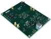
Evaluation Kit for 9FGV1005 Programmable PhiClock™ Generator
This is the evaluation board for the 9FGV1005 programmable PhiClockTM generator. It provides a convenient way of configuring and programming the blank parts for the...

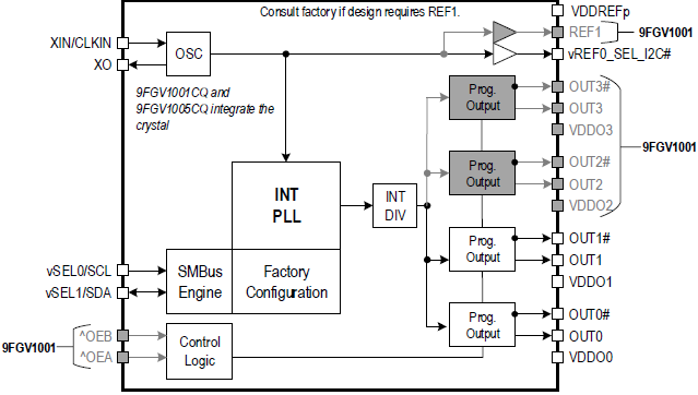
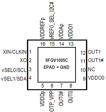
The 9FGV1005 is a member of Renesas' PhiClock™ programmable clock generator family. The 9FGV1005 provides 2 copies of a single non-spread spectrum output frequency and one copy of the crystal reference input. Two select pins allow for hardware selection of the desired configuration, or two I²C bits all easy software selection of the desired configuration. The user may configure any one of the four OTP configurations as the default when operating in I²C mode. Four unique I²C addresses are available, allowing easy I²C access to multiple components.
This is the evaluation board for the 9FGV1005 programmable PhiClockTM generator. It provides a convenient way of configuring and programming the blank parts for the...
This is the evaluation board for the 9FGV1005Q5 programmable PhiClockTM generator with internal 50MHz crystal. It provides a convenient way of configuring and...
Schematic symbols, PCB footprints, and 3D CAD models from SamacSys can be found by clicking on products in the Product Options table. If a symbol or model isn't available, it can be requested directly from the website.

Output Type |
Output Freq Range (MHz) |
Supply Voltage (V) |
Xtal Freq (MHz) |
Carrier Type |
Moisture Sensitivity Level (MSL) |
Price (USD) | 1ku |
Buy / Sample |
|
|---|---|---|---|---|---|---|---|---|
| Part Number | ||||||||
| LP-HCSL | 50, 100, 125, 156.25 | 3.3 | 25 | Tray | 3 | Get Samples, | ||
| LP-HCSL | 50, 100, 125, 156.25 | 3.3 | 25 | Reel | 3 | |||
| LP-HCSL | 50, 100, 125, 156.25 | 1.8 | 25 | Tray | 3 | Get Samples, | ||
| LP-HCSL | 50, 100, 125, 156.25 | 1.8 | 25 | Reel | 3 | |||
| LP-HCSL | 161.1328125, 312.5, 322.265625, 156.25 | 3.3 | 39.0625 | Tray | 3 | Get Samples, | ||
| LP-HCSL | 161.1328125, 312.5, 322.265625, 156.25 | 3.3 | 39.0625 | Reel | 3 | |||
| LP-HCSL | 161.1328125, 312.5, 322.265625, 156.25 | 1.8 | 39.0625 | Tray | 3 | Get Samples, | ||
| LP-HCSL | 161.1328125, 312.5, 322.265625, 156.25 | 1.8 | 39.0625 | Reel | 3 | |||
| LP-HCSL | 50, 100, 125, 156.25 | 3.3 | 50 | Tray | 3 | 3.736 | Get Samples, | |
| LP-HCSL | 50, 100, 125, 156.25 | 3.3 | 50 | Reel | 3 | |||
| LP-HCSL | 50, 100, 125, 156.25 | 1.8 | 50 | Tray | 3 | 3.736 | Get Samples, | |
| LP-HCSL | 50, 100, 125, 156.25 | 1.8 | 50 | Reel | 3 |

IDT’s chief PCIe system architect explains the fundamental difference in reference clock jitter budgets between the first three generations of the specification and those of Gen4 and Gen5 which raise new challenges for designers.
| Blog Post | Apr 14, 2022 | ||
| Blog Post | Jun 14, 2019 | ||
| Blog Post | May 22, 2018 | ||
| News | Apr 30, 2018 |