6-output 1.8 V PCIe Gen1-4 Clock Generator
Jump to Page Section:
Overview
Description
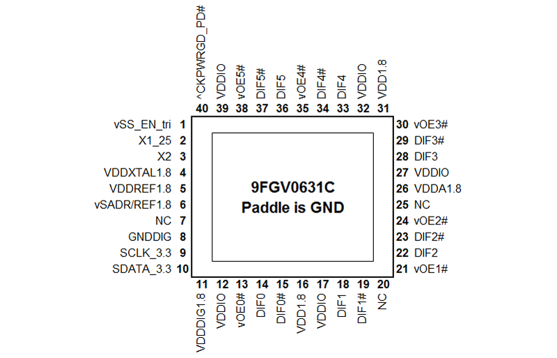
The 9FGV0631 is a member of IDT's SOC-Friendly 1.8 V Very-Low-Power PCIe clock family. The device has 6 output enables for clock management, 2 different spread spectrum levels in addition to spread off and 2 selectable SMBus addresses.

Features
-
PCIe Gen1–4 compliant
-
LP-HCSL outputs; save 12 resistors compared to standard PCIe devices
-
54 mW typical power consumption; reduced thermal concerns
-
Outputs can optionally be supplied from any voltage between 1.05 and 1.8 V; maximum power savings
-
OE# pins; support DIF power management
-
Programmable slew rate for each output; allows tuning for various line lengths
-
Programmable output amplitude; allows tuning for various application environments
-
DIF outputs blocked until PLL is locked; clean system start-up
-
Selectable 0%, -0.25% or -0.5% spread on DIF outputs; reduces EMI
-
External 25 MHz crystal; supports tight ppm with 0 ppm synthesis error
-
Configuration can be accomplished with strapping pins; SMBus interface not required for device control
-
3.3 V tolerant SMBus interface works with legacy controllers
-
Space saving 5x5 mm 40-pin VFQFPN; minimal board space
-
Selectable SMBus addresses; multiple devices can easily share an SMBus segment
Comparison
Applications
Design & Development
Models
ECAD Models
Schematic symbols, PCB footprints, and 3D CAD models from SamacSys can be found by clicking on products in the Product Options table. If a symbol or model isn't available, it can be requested directly from the website.

Processing table
| VFQFPN | 40 | I | Yes | Tray | ||
| VFQFPN | 40 | I | Yes | Reel | ||
| VFQFPN | 40 | C | Yes | Tray | ||
| VFQFPN | 40 | C | Yes | Reel |

Tips for Using This Parametric Table:
- Hide Filters button in header: Collapse or expands filters
- Column sort buttons in header: Sort Column alphabetically / numerically descending or ascending
- Reset button in header: Reset all filters to the page default
- Full Screen button in header: Expand the table to full screen view (user must close out of full screen before they can interact with rest of page)
- Export button in header: Export the filtered results of the table to an Excel document
- Filter parts search bar in header: Type to filter table results by part number
- Hide column button in column headers: Select to hide columns in table
- AND / OR toggle switches in header: Toggles the logic of this particular filter to be “AND” or “OR” logic for filtering results
- Multiselect checkboxes at beginning of each row in table: Select these checkboxes to compare products against each other
- Document icon next to product name in row: View the featured document for this product
- Chip icon next to the right of the document icon in row: View the block diagram for this product
- Cart icon to the right of the chip icon: Indicates that samples are available for this product
Videos & Training
PCIe Reference Clock Jitter Budgets
IDT’s chief PCIe system architect explains the fundamental difference in reference clock jitter budgets between the first three generations of the specification and those of Gen4 and Gen5 which raise new challenges for designers.
Video List
News & Blog Posts
| Blog Post | Apr 14, 2022 | ||
| Blog Post | May 22, 2018 | ||
| News | Apr 30, 2018 |