
Overview
Description
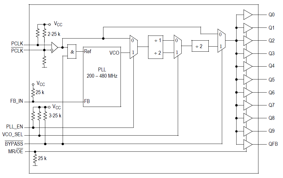
The MPC9658 utilizes PLL technology to frequency lock its outputs onto an input reference clock. Normal operation of the MPC9658 requires the connection of the QFB output to the feedback input to close the PLL feedback path (external feedback). With the PLL locked, the output frequency is equal to the reference frequency of the device and VCO_SEL selects the operating frequency range of 50 to 125 MHz or 100 to 250 MHz. The two available post-PLL dividers selected by VCO_SEL (divide-by-2 or divide-by-4) and the reference clock frequency determine the VCO frequency. Both must be selected to match the VCO frequency range. The internal VCO of the MPC9658 is running at either 2x or 4x of the reference clock frequency. The MPC9658 has a differential LVPECL reference input along with an external feedback input. The MPC9658 is ideal for use as a zero delay, low skew fanout buffer. The device performance has been tuned and optimized for zero delay performance. The PLL_EN and BYPASS controls select the PLL bypass configuration for test and diagnosis. In this configuration, the selected input reference clock is bypassing the PLL and routed either to the output dividers or directly to the outputs. The PLL bypass configurations are fully static and the minimum clock frequency specification and all other PLL characteristics do not apply. The outputs can be disabled (high-impedance) and the device reset by asserting the MR/OE pin. Asserting MR/OE also causes the PLL to loose lock due to missing feedback signal presence at FB_IN. Deasserting MR/OE will enable the outputs and close the phase locked loop, enabling the PLL to recover to normal operation. The MPC9658 is fully 3.3 V compatible and requires no external loop filter components. The inputs (except PCLK) accept LVCMOS except signals while the outputs provide LVCMOS compatible levels with the capability to drive terminated 50 ? transmission lines. For series terminated transmission lines, each of the MPC9658 outputs can drive one or two traces giving the devices an effective fanout of 1:16. The device is packaged in a 7x7 mm2 32-lead LQFP package.
Features
- Low based low-voltage clock generator
- Supports zero-delay operation
- 3.3 V power supply
- Generates clock signals up to 250 MHz
- Maximum output skew of 120 ps
- Differential LVPECL reference clock input
- External PLL feedback
- Drives up to 20 clock lines
- 32-lead LQFP packaging
- 32-lead Pb-free Package Available
- Pin and function compatible to the MPC958
Comparison
Applications
Design & Development
Models
ECAD Models
Schematic symbols, PCB footprints, and 3D CAD models from SamacSys can be found by clicking on products in the Product Options table. If a symbol or model isn't available, it can be requested directly from the website.

Processing table
| TQFP | 32 | C | Yes | Tray |

Tips for Using This Parametric Table:
- Hide Filters button in header: Collapse or expands filters
- Column sort buttons in header: Sort Column alphabetically / numerically descending or ascending
- Reset button in header: Reset all filters to the page default
- Full Screen button in header: Expand the table to full screen view (user must close out of full screen before they can interact with rest of page)
- Export button in header: Export the filtered results of the table to an Excel document
- Filter parts search bar in header: Type to filter table results by part number
- Hide column button in column headers: Select to hide columns in table
- AND / OR toggle switches in header: Toggles the logic of this particular filter to be “AND” or “OR” logic for filtering results
- Multiselect checkboxes at beginning of each row in table: Select these checkboxes to compare products against each other
- Document icon next to product name in row: View the featured document for this product
- Chip icon next to the right of the document icon in row: View the block diagram for this product
- Cart icon to the right of the chip icon: Indicates that samples are available for this product