2.5 V to 3.3 V 1:6 TCXO / LVCMOS High-Performance Clock Buffer
Jump to Page Section:
Overview
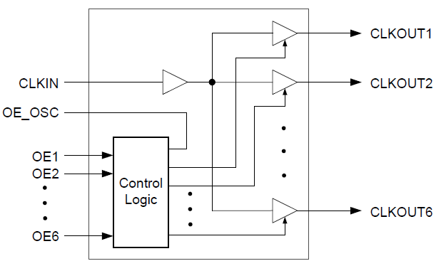
Description
The 5PB1216 is a high-performance TCXO / LVCMOS clock fanout buffer with individual OE pin for each output. The CLKIN pin can accept either a square wave (LVCMOS) or clipped sine wave (such as TCXO clipped sine wave output) as input.
The 5PB1216 has industry-leading low jitter and extremely low current consumption, making it ideal for smart mobile devices.
The 5PB1216 has industry-leading low jitter and extremely low current consumption, making it ideal for smart mobile devices.
Features
- Extremely low operating and standby current consumption
- Low RMS Additive Phase jitter
- 2.5 V to 3.3 V power supply voltage
- Six outputs with individual Output Enable pin
- One input
- OE_OSC control pin to enable/disable reference TCXO / XO
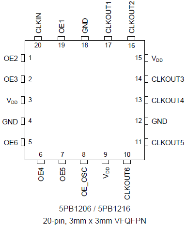
- Small 20-pin VFQFPN package
- Extended temperature range (-40°C to +105°C)
Comparison
Applications
Design & Development
Models
ECAD Models
Schematic symbols, PCB footprints, and 3D CAD models from SamacSys can be found by clicking on products in the Product Options table. If a symbol or model isn't available, it can be requested directly from the website.

Processing table
| VFQFPN | 20 | K | Yes | Tray | 1 | 1.995 | Get Samples, | |
| VFQFPN | 20 | K | Yes | Reel | 1 |

Tips for Using This Parametric Table:
- Hide Filters button in header: Collapse or expands filters
- Column sort buttons in header: Sort Column alphabetically / numerically descending or ascending
- Reset button in header: Reset all filters to the page default
- Full Screen button in header: Expand the table to full screen view (user must close out of full screen before they can interact with rest of page)
- Export button in header: Export the filtered results of the table to an Excel document
- Filter parts search bar in header: Type to filter table results by part number
- Hide column button in column headers: Select to hide columns in table
- AND / OR toggle switches in header: Toggles the logic of this particular filter to be “AND” or “OR” logic for filtering results
- Multiselect checkboxes at beginning of each row in table: Select these checkboxes to compare products against each other
- Document icon next to product name in row: View the featured document for this product
- Chip icon next to the right of the document icon in row: View the block diagram for this product
- Cart icon to the right of the chip icon: Indicates that samples are available for this product
Videos & Training
5PB11xx Ultra Low Jitter LVCMOS Buffers
This video provides an overview of the LVCMOS High Performance Clock Buffer Family, highlighting their key features and capabilities.

Video List
News & Blog Posts
| News | Mar 24, 2015 |