
Wide-Range Transmission Output Control and Reduced Transmitter Noise Realized Dynamic Range of 78 dB, Power Control Accuracy of 0.27 dB, and Low Transmitter Noise of −160.4 dBc/Hz
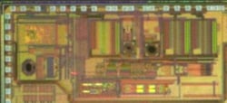 Renesas Electronics' prototype using CMOS programmable gain amplifier circuit technology
TOKYO, Japan, June 18, 2010 — Renesas Electronics Corporation (TSE: 6723) today announced the development of CMOS programmable gain amplifier (PGA) circuit technology combining wide-range transmission output control and low transmitter noise (Note 1) for the transmitter circuit block. This new technology is suitable for multi-mode radio frequency integrated circuit (RF transceiver IC) devices with support for multiple wireless standards, such as W-CDMA (Note 2) and the LTE (Note 3) next-generation high-speed data communication standard.
The new technology makes it possible to realize amplifiers with wide-range, highly accurate power control in a single stage, rather than multiple stages as were previously needed, by making modifications to the circuit structure of amplifiers. This reduces the transmitter noise generated by each amplifier and eliminates the existing need for a SAW filter (Note 4) to suppress such noise, enabling more compact system design.
In addition, Renesas Electronics succeeded in a prototype of PGA using a 65 nanometer (nm) CMOS process and the new technology that achieved a 78 dB dynamic range, precise power control accuracy of 0.27 dB, and transmitter noise of only −160.4 dBc/Hz, which is so low that a SAW filter is unnecessary. The prototype also has low power consumption at low gain levels.
In recent years, there has been an increasing demand for mobile wireless handsets with international roaming functionality, which enables the transfer of data and making of calls anywhere in the world. In order to provide for this demand, handset makers use multi-mode/multi-band RF transceiver ICs that support many communication standards, such as GSM (Note 5), W-CDMA, and LTE, as well as multiple frequency bands. However, since multi-mode/multi-band RF transceiver ICs require more SAW filters connected to the transmitter circuit output stage, the mounting area and overall cost of mobile wireless handsets increase. This has therefore spurred demand for reduced transmitter noise in order to eliminate the need for SAW filters to suppress such noise.
The W-CDMA and LTE standards call for a 74 dB dynamic range and transmission output power control in 1 dB steps. This is to enable base stations to accommodate as many users as possible by controlling the output power so that users close to a base station transmit at lower power and users farther away from a base station transmit at higher power. This transmission power control is performed by a PGA using analog/digital control signals. PGAs employing conventional circuit technology achieve a 74 dB dynamic range by using three amplifier stages in a cascade arrangement, with each stage capable of controlling a dynamic range of 20 to 30 dB. However, in such configuration the noise generated by the earlier stages is amplified by the subsequent stages, making it difficult to keep transmitter noise at a low enough level.
The newly developed CMOS PGA circuit technology using a new circuit configuration achieves both wide-range transmission output power control and low transmitter noise, two goals that have been extremely difficult to achieve when using conventional CMOS circuit technology.
The key features and details of the new technology are described below.
1. Development of a gain control method providing wide dynamic range and precise gain steps in a single-stage configuration
The newly developed gain control method uses 18 amplifiers (6 dB step amplifiers) having common I/O terminals and each with gain that increases by one-half (6 dB) compared with the one preceding it. Digital signals are used for on/off control of the individual amplifiers. The total voltage gain is the sum of the voltage gains of the amplifiers that are switched on. Switching control works as follows.
(1) Large step control up to 78 dB is accomplished by switching 13 (78 dB ÷ 6 dB) units of 6 dB step amplifiers.
(2) Fine step control between the 6 dB steps of (1) above is accomplished by on/off switching of five consecutive 6 dB step amplifiers.
Combining (1) and (2) above would seem to require a total of 65 (13 × 5) units of 6 dB step amplifiers. However, since all are 6 dB step amplifiers, the actual number required is 18 (13 + 5) units. In addition, shared use of the amplifiers prevents degradation in gain control accuracy due to inconsistency in the properties of individual elements.
2. Implementation of the new gain control method in a circuit configuration with reduced power consumption
To realize a CMOS circuit using the gain control method, the 18 units of 6 dB step amplifiers are combined with voltage-current converters and a resistive attenuator. Gain loss due to the parasitic capacitance of elements and wiring is a factor that must be taken into account in RF signal processing, so care has been needed in configuring the 6 dB step amplifiers. In addition, the RF transceiver IC requires large currents at high gain levels, but it needs to maintain low current consumption to reduce power consumption at low gain levels.
To get around these two issues, the following two configuration elements are used together.
(1) An R-2R resistive ladder attenuator is used to enable highly accurate 6 dB step voltage attenuation even in the RF band.
(2) To reduce current consumption at low gain levels, the upper four 6 dB step amplifiers are connected in parallel to eight, four, two, and one identical voltage-current converter, respectively.
These configuration elements make it possible to build a single-stage amplifier that achieves a dynamic range of 78 dB, gain control accuracy of 0.27 dB, and low power consumption at low gain levels.
The new technology is expected to contribute to the realization of future multi-mode RF transceiver IC products that require no SAW filters.
Renesas Electronics views these new technologies as a cornerstone in realization of future multi-mode RF transceiver IC products that require no SAW filters.
Renesas Electronics presented the results of this research at the Symposium on VLSI Circuits, which was held in Honolulu, Hawaii from June 16 to June 18.
(Note 1) Transmitter noise: Noise in the reception band output by the transmitter circuit block of the RF transceiver IC.
(Note 2) W-CDMA (Wideband Code Division Multiple Access): A third-generation mobile communication standard established by the 3rd Generation Partnership Project (3GPP) standards body.
(Note 3) LTE (Long Term Evolution): A next-generation high-speed mobile communication standard promoted by the 3GPP.
(Note 4) SAW (surface acoustic wave) filter: A filter consisting of a piezoelectric substrate with comb electrodes arranged on it in a spacing that allows only the desired wavelength to pass though.
(Note 5) GSM (Global System for Mobile Communications): A communication standard used in second-generation mobile phones.
About Renesas Electronics Corporation
Renesas Electronics Corporation (TSE: 6723) delivers trusted embedded design innovation with complete semiconductor solutions that enable billions of connected, intelligent devices to enhance the way people work and live. A global leader in microcontrollers, analog, power and SoC products, Renesas provides comprehensive solutions for a broad range of automotive, industrial, infrastructure, and IoT applications that help shape a limitless future. Learn more at renesas.com. Follow us on LinkedIn, Facebook, Twitter, and YouTube.
The content in the press release, including, but not limited to, product prices and specifications, is based on the information as of the date indicated on the document, but may be subject to change without prior notice.