
1:2 Fanout Buffer With Pre-Emphasis
Jump to Page Section:
Overview
Description
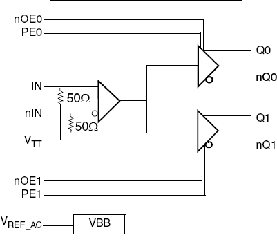
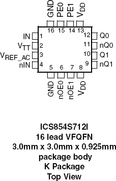
The 854S712I is a differential, high-speed 1:2 data/clock fanout buffer and line driver. The outputs support pre-emphasis in order to drive backplanes and long transmission lines while reducing inter-symbol interference effects. The pre-emphasis level is configurable to optimize for low bit error rate or power consumption. Pre-emphasis utilizes an increased output voltage swing for transition bits. The device is optimized for data rates up to 4.5 Gbps (NRZ) and for deterministic jitter in data applications and low additive jitter in clock applications. The outputs are LVDS-compliant while the differential input is compatible with a variety of signal levels such as LVDS, LVPECL and CML. Internal input termination, a bias voltage output for AC-coupling and small packaging (VFQFN) supports space-efficient board designs. The 854S712I operates from a 3.3V power supply and supports the industrial temperature range of -40°C to +85°C.
Features
- 1:2 differential data/clock fanout buffer and line driver
- 4.5 Gbps data rate (NRZ) (maximum)
- Differential LVDS outputs
- Differential input supporting LVDS, LVPECL and CML levels
- Configurable output pre-emphasis
- Low-skew outputs: 10ps (maximum)
- Low data deterministic jitter: 4ps (maximum)
- LVCMOS interface levels for the control inputs
- Asynchronous output disable into high-impedance state
- Internal input termination: 100? (Differential)
- Additive phase jitter, RMS: 0.08ps (typical)
- Full 3.3V supply voltage
- -40°C to 85°C ambient operating temperature
- Available in lead-free (RoHS 6) package
Comparison
Applications
Design & Development
Models
ECAD Models
Schematic symbols, PCB footprints, and 3D CAD models from SamacSys can be found by clicking on products in the Product Options table. If a symbol or model isn't available, it can be requested directly from the website.

Processing table
| VFQFPN | 16 | I | Yes | Tray | 3 | 7.593 | Get Samples, | |
| VFQFPN | 16 | I | Yes | Reel | 3 |

Tips for Using This Parametric Table:
- Hide Filters button in header: Collapse or expands filters
- Column sort buttons in header: Sort Column alphabetically / numerically descending or ascending
- Reset button in header: Reset all filters to the page default
- Full Screen button in header: Expand the table to full screen view (user must close out of full screen before they can interact with rest of page)
- Export button in header: Export the filtered results of the table to an Excel document
- Filter parts search bar in header: Type to filter table results by part number
- Hide column button in column headers: Select to hide columns in table
- AND / OR toggle switches in header: Toggles the logic of this particular filter to be “AND” or “OR” logic for filtering results
- Multiselect checkboxes at beginning of each row in table: Select these checkboxes to compare products against each other
- Document icon next to product name in row: View the featured document for this product
- Chip icon next to the right of the document icon in row: View the block diagram for this product
- Cart icon to the right of the chip icon: Indicates that samples are available for this product