画像


Renesasが提供するPCIe® Gen3用リタイマの製品ファミリは、最高レベルのアナログ性能と少ない消費電力を実現しています。また、要求の厳しいコンピュータ、ストレージ、通信といった分野で、2.5Gbps、5Gbps、8Gbpsの伝送速度を必要とするアプリケーション向けに最適化されたシステムレベルの信号リタイマ機能の大半を提供しています。
RenesasのPCIe用リタイマは以下のような機能を備えています。
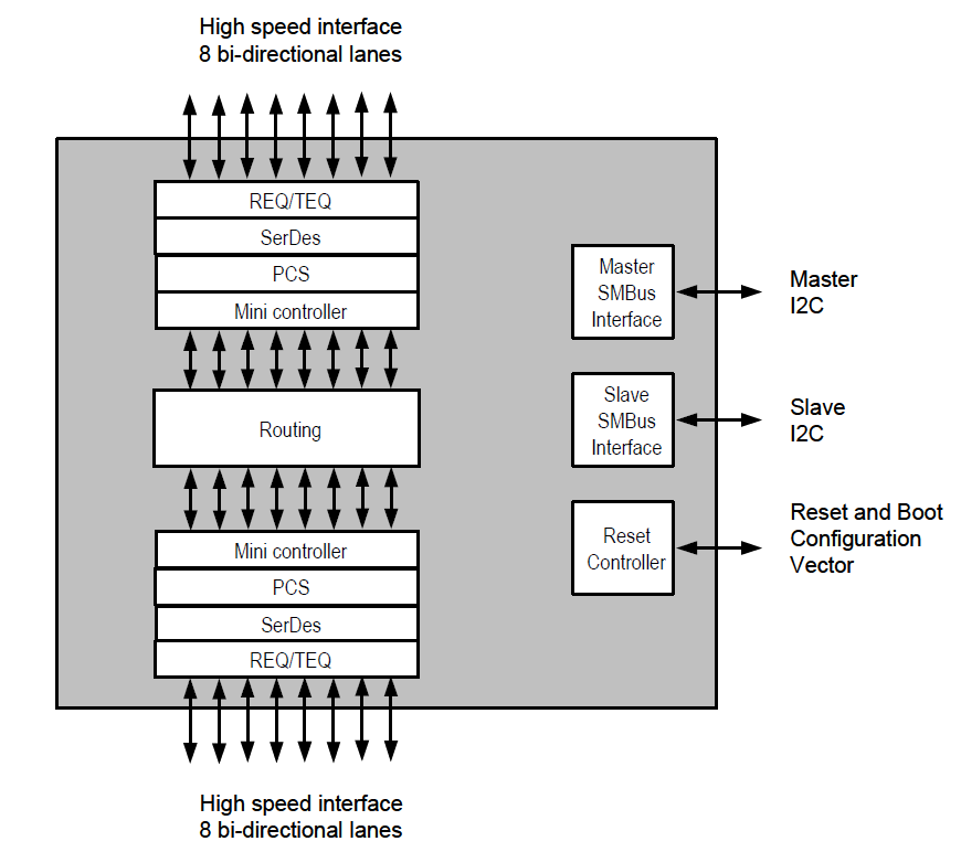
RenesasのPCIe用リタイマ(シグナルコンディショナ)は、ケーブルやプリント基板のトレースが長いシステムの性能と信頼性を向上し、シグナルインテグリティを確保するために使用します。また、入力信号からランダムジッターと確定的ジッターを取り除いてシンボル間干渉を排除し、出力ジッターバジェットをリセットします。RenesasのPCIe用リタイマには、8GT/s(Transfer/sec)のPCI Express 3.0に対応する差動チャンネルを8/16/32系統備えるデバイスが用意されており、それぞれ4/8/16レーンに対応しています。また、5GT/s、2.5GT/sのPCI Expressの機能をすべてサポートしています。
RenesasのPCIe用リタイマは、CDR(クロックデータリカバリ)アーキテクチャ、適応型のDFE(Decision Feedback Equalizer)、シリアルインタフェースによってアクセスされる多様な制御オプションで構成されています。各チャンネルに小型コントローラを備えており、イコライゼーションのトレーニングを行ったうえで、自動調節によって最高の性能が得られるよう自己構成が行えます。小型コントローラは、各リンクについて、128b/130bによる符号化、PCIe Gen1/2との互換性を保つためのダウンシフト、レシーバの検出、終端制御などの機能の制御を行います。
RenesasのPCIe用リタイマは、いずれも非線形/適応型の多段イコライザ、アナログフロントエンド、5タップのDFEを搭載しています。DFEの帰還フィルタは、前のシンボルからのISI(Inter-symbol Interference)歪みを完全に取り除き、デジタルイコライゼーションによってフィルタの出力のノイズを除去します。フィルタのタップに対する重みづけは、構成用のシリアルインタフェースによって調整できます。
イコライザ、ディエンファシス、送信信号のフルスケール振幅のデフォルト値は、ピンプログラマブルに設定可能です。PCIe用リタイマはSMBusやI2Cのスレーブデバイスとして機能させることができます。その場合、各インタフェースによってあらゆる機能/動作の構成が行えます。マスターモードで動作させれば、構成用のデータをEEPROMからダウンロードできます。また、シリアルバスによって多くのステータスレジスタを確認することも可能です。
PCIe用リタイマの信号終端はデフォルトでは100Ω(公称値)に設定されています。これは、必要に応じて85Ω(公称値)にプログラムすることも可能です。入力信号の検出に使うしきい値は、有効な信号のレベルに応じて調節できるとともに、アイドリング信号をサポートします。
また、RenesasのPCIe用リタイマは、基板のテストを容易に行えるようにするために、JTAG/AC JTAGをサポートしています。加えて、実験やフィールドテストを容易化できるようパターンジェネレータも内蔵しています。さらにはテスト/デバッグ用に、デバイスの構成情報を設定/保存するためのPC向けユーティリティや、遠隔でのフィールド診断を支援するアイダイアグラムのキャプチャツールなど、さまざまなソフトウェアも用意されています。
リタイマICは、電源電圧として1.0V、1.8V、3.3Vを使用します。また、各リンクのASPM(Active State Power Management)など、省電力化に向けたさまざまな機能も備えています。
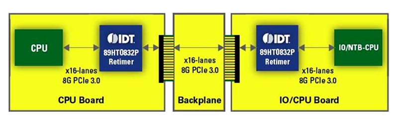
高速信号の品質は、トランスミッタ、レシーバ、チャンネルの特性が原因で、最終的にレシーバに到達するまでに、許容できないレベルにまで低下する場合があります。PCIe用リタイマは、ケーブルやプリント基板のトレースにおける減衰とISI(Inter-symbol Interference)ジッターを補償し、ターゲットとなるレシーバにおけるジッターを最小化してアイの開きを最大化します。これは、送信信号を増幅するか、受信信号をイコライズするかによって行われます。チャンネル長が長かったり、ビアやコネクタによって不連続性が生じていたりするためにいずれか一方だけでは十分な効果が得られない場合には両方が適用されます。Renesas社のリタイマICは、ブレードサーバー、エンタープライズ向けストレージ、通信システム、クラウドコンピューティングなどのアプリケーションにおけるシグナルインテグリティの課題を解決するうえで最適な製品となっています。
| PCIe Gen3 Signal Retimer | 16 | PCIe | 8 | FCBGA | 15.0 x 15.0 x 2.6 | C, I |
| 16-lane, 8 Gbps, PCIe 3.0 Retimer | 32 | PCIe | 8 | FCBGA | 13.0 x 20.0 x 2.84, 24.0 x 15.5 x 2.8 | C, I |
Description
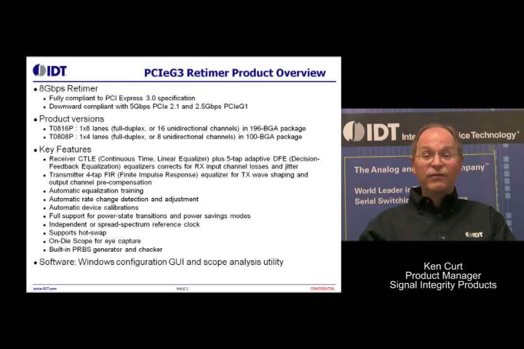
The IDT PCI Express 3.0 Retimer supports high-speed signal conditioning up to 8Gbps, enhancing signal quality over long distances and simplifying design by reducing board layout constraints. These devices incorporate advanced receive equalization and transmit de-emphasis capabilities, as well as diagnostic features that help IDT customers achieve a simplified design with faster time-to-market. The devices all offer power savings modes for the lowest-possible power consumption. Presented by Ken Curt, Product Manager, Integrated Device Technology, Inc. Learn more at by visiting the PCI Express® Gen3 Retimers page.
Transcript