Evaluation Kit for 9FGV1004 Programmable PhiClock™ Generator
This is the evaluation board for the 9FGV1004 programmable PhiClock™ generator. It provides a convenient way of configuring and programming the blank parts for the...

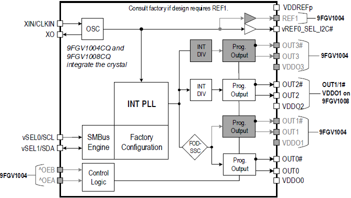
9FGV1004は、ルネサスのPhiClock™プログラマブルクロックジェネレータファミリのひとつです。 9FGV1004は、整数に関連する2つの周波数が各1コピー、フラクショナルまたはスペクトラム拡散の周波数が2コピー、水晶振動子のリファレンス入力が2コピー用意されています。 2つの選択ピンでハードウェア的に、または2つのI²Cビットでソフトウェア的に、簡単にかつ希望のコンフィギュレーションで選択することができます。 I²Cモードで動作させる場合、ユーザーは4つのOTPコンフィギュレーションから1つをデフォルトとして設定することができます。 4つのユニークI²Cアドレスが利用可能で、複数のコンポーネントに簡単にI²Cアクセスすることができます。
This is the evaluation board for the 9FGV1004 programmable PhiClock™ generator. It provides a convenient way of configuring and programming the blank parts for the...
[製品選択]テーブル内の製品名をクリックするとSamacSysが提供する回路図シンボル、PCBフットプリント、3D CADモデルがご確認いただけます。 お探しのシンボルやモデルが見つからない場合、Webサイトから直接リクエストできます。


IDT’s chief PCIe system architect explains the fundamental difference in reference clock jitter budgets between the first three generations of the specification and those of Gen4 and Gen5 which raise new challenges for designers.
| ブログ | 2022年4月14日 | ||
| ブログ | 2019年6月14日 | ||
| ブログ | 2018年5月22日 | ||
| ニュース | 2018年4月30日 |