
概览
简介
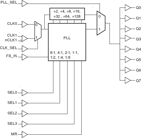
The 8705I is a highly versatile 1:8 Differential-to- LVCMOS/LVTTL Clock Generator. The 8705I has two selectable clock inputs. The CLK1, nCLK1 pair can accept most standard differential input levels. The single ended CLK0 input accepts LVCMOS or LVTTL input levels. The 8705I has a fully integrated PLL and can be configured as zero delay buffer, multiplier or divider and has an input and output frequency range of 15.625MHz to 250MHz. The reference divider, feedback divider and output divider are each programmable, thereby allowing for the following output-to-input frequency ratios: 8:1, 4:1, 2:1, 1:1, 1:2, 1:4, 1:8. The external feedback allows the device to achieve "zero delay" between the input clock and the output clocks. The PLL_SEL pin can be used to bypass the PLL for system test and debug purposes. In bypass mode, the reference clock is routed around the PLL and into the internal output dividers.
特性
- Eight LVCMOS/LVTTL outputs, 7Ω typical output impedance
- Selectable CLK1, nCLK1 or LVCMOS/LVTTL clock inputs
- CLK1, nCLK1 pair can accept the following differential input levels: LVPECL, LVDS, LVHSTL, HCSL, SSTL
- CLK0 input accepts LVCMOS or LVTTL input levels
- Output frequency range: 15.625MHz to 250MHz
- Input frequency range: 15.625MHz to 250MHz
- VCO range: 250MHz to 500MHz
- External feedback for "zero delay" clock regeneration with configurable frequencies
- Programmable dividers allow for the following output-to-input frequency ratios: 8:1, 4:1, 2:1, 1:1, 1:2, 1:4, 1:8
- Fully integrated PLL
- Cycle-to-cycle jitter: 45ps (maximum)
- Output skew: CLK0, 65ps (maximum) CLK1, nCLK1, 55ps (maximum)
- Static Phase Offset: 25 ±125ps (maximum), CLK0
- Full 3.3V or 2.5V operating supply
- Lead-Free package available
- -40°C to 85°C ambient operating temperature
产品对比
应用
设计和开发
模型
ECAD 模块
Schematic symbols, PCB footprints, and 3D CAD models from SamacSys can be found by clicking on products in the Product Options table. If a symbol or model isn't available, it can be requested directly from the website.

Processing table
| TQFP | 32 | I | Yes | Tray | ||
| TQFP | 32 | I | Yes | Reel |

Tips for Using This Parametric Table:
- Hide Filters button in header: Collapse or expands filters
- Column sort buttons in header: Sort Column alphabetically / numerically descending or ascending
- Reset button in header: Reset all filters to the page default
- Full Screen button in header: Expand the table to full screen view (user must close out of full screen before they can interact with rest of page)
- Export button in header: Export the filtered results of the table to an Excel document
- Filter parts search bar in header: Type to filter table results by part number
- Hide column button in column headers: Select to hide columns in table
- AND / OR toggle switches in header: Toggles the logic of this particular filter to be “AND” or “OR” logic for filtering results
- Multiselect checkboxes at beginning of each row in table: Select these checkboxes to compare products against each other
- Document icon next to product name in row: View the featured document for this product
- Chip icon next to the right of the document icon in row: View the block diagram for this product
- Cart icon to the right of the chip icon: Indicates that samples are available for this product