图像


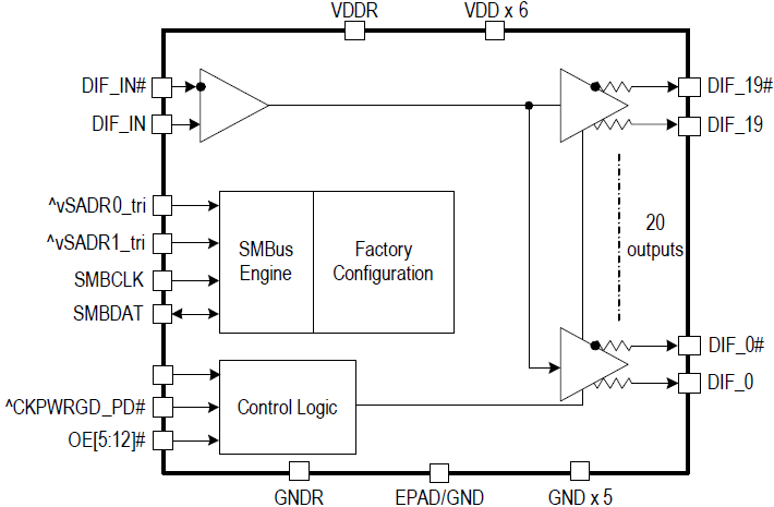
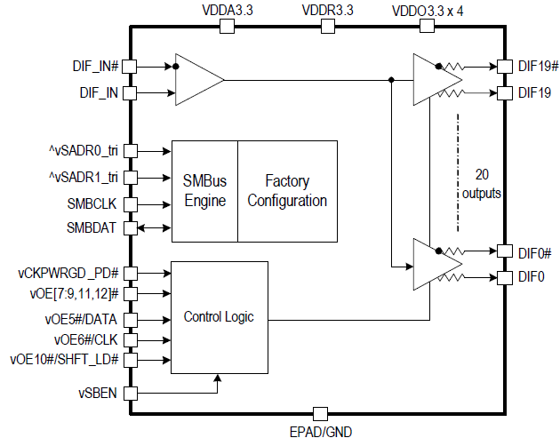
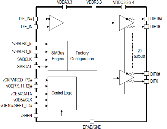
零延迟缓冲器 (ZDB) 提供了输出端输入时钟的同步拷贝(无传播延迟),并且一般情况下无需转换频率。 Renesas’ 的 ZDB 均是基于 PLL 的器件,可重新生成带扇出的输入时钟信号,以驱动多个负载提供多种信号级,包括 LVPECL、LVDS、HCSL、CML、HSTL、SSTL 或 LVCMOS。 对于 FPGA、CPU、逻辑和同步存储器等需要同步时钟的应用而言,ZDB 是它们的理想选择。
大多数零延迟缓冲器的延迟可通过外部反馈路径进行调节。 这样可以实现对时钟信号到达负载所需计时的精确控制。 当全部输出(包括反馈输出)均采用简单分频器时,可进行简单的频率转换以保持时钟同步化。
提示: 如果需要不止一个唯一的输出频率(如 100MHz 和 125MHz),可使用“输出库”参数选择器。 每个库与唯一的输出频率对应。
Renesas' 的零延迟缓冲器 (ZDB) 产品系列拥有广泛的选项和功能。 LVPECL、LVDS、HCSL、CML、HSTL、SSTL 和可选输出等差分输出,都支持高达 3.2GHz 的输出频率和频率高达 350MHz 的单端 LVCMOS 输出。 此外,Renesas' 的 PLL 产品组合中有一些器件支持 1.2V 至 5V 电源电压,可在商业和工业温度范围内使用。
使用 Renesas PLL 产品具有多种好处。 减少电路板上石英晶体的数量,从而提高可靠性,因为晶体很容易受到冲击和振动的影响。 使用时钟信号发生器后,通过使用一个器件取代多个晶体和振荡器,还可降低消费类电子产品'的电路板成本和空间、材料单 (BOM) 和库存水平。 对于包括个人电脑、消费类电子产品或工业系统,以及高性能网络和通信系统在内的各种系统而言,它们都是理想选择。
选择用于特定应用的 ZDB 时要考虑许多重要因素。 用户可以下列参数作为起始点,来缩小潜在解决方案的范围:
Outputs (#) |
Output Type |
Output Freq Range (MHz) |
Input Freq (MHz) |
Inputs (#) |
Input Type |
Output Banks (#) |
Core Voltage (V) |
Output Voltage (V) |
Divider Value |
|
|---|---|---|---|---|---|---|---|---|---|---|
| 器件号 | ||||||||||
| 20-Output DB2000Q PCIe Clock Buffer | 20 | LP-HCSL | 1 - 400 | 1 - 400 | 1 | HCSL | 1 | 3.3 | 0.7 | |
| 20-Output Enhanced DB2000Q PCIe Clock Buffer | 20 | LP-HCSL | 1 - 400 | 1 - 400 | 1 | HCSL | 1 | 3.3 | 0.7 | |
| 20-Output DB2000QL PCIe Clock Buffer | 20 | LP-HCSL | 1 - 400 | 1 - 400 | 1 | HCSL | 1 | 3.3 | 0.7 | |
| 20-Output Enhanced DB2000QL PCIe Clock Buffer | 20 | LP-HCSL | 1 - 400 | 1 - 400 | 1 | HCSL | 1 | 3.3 | 0.7 |
Description
Brief overview of IDT's zero-delay buffers. Zero-delay buffers (ZDB) are ideal for applications requiring synchronized clocking for FPGAs, CPUs, logic, and synchronous memory. Zero-delay buffers are PLL-based devices that regenerate the input clock signal with fanout to drive multiple loads. Most devices allow the delay through the device to be adjusted through an external feedback path. This allows precise control of the timing of the clock signals to the loads. Zero-delay buffers provide a synchronous copy of the input clock at the outputs, usually without frequency translation. Simple frequency translation is possible when a single divider is used for all outputs, including feedback output, to maintain clock synchronization. Presented by Vik Chaudhry, technical marketing manager at IDT. For more visit the Zero Delay Buffers page.
Transcript