

An "FPGA microcontroller" enables you to realize the functions of a general-purpose microcontroller in an FPGA. We introduce FPGA microcontrollers via a link from our web page for IP products and blogs. Now, to give you a deeper understanding, we’ll introduce the activities of Renesas for realizing microcontrollers in FPGAs.
In the design of H8S products, the method was changed to RTL design from the initial stages into the 2000s. The CPUs described at the RTL are implemented as the actual H8S microcontroller products. As embedding small processors became required in the in-house development of application-specific standard products (ASSPs) following the RTL description of the CPUs, Renesas prepared the H8S C200 core for inclusion as the CPU along with other standard microcontroller functions. The H8S C200 core is now offered as an IP product and is incorporated into and used in many devices manufactured in-house with various processes even today. The provision of design data for H8S products under IP licenses was also started in the 2000s.
Activities for Applying the H8S C200 Core IP in an FPGA
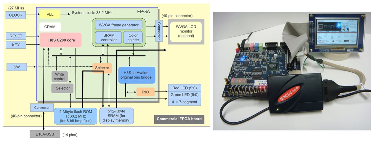
For ease of usability in various devices, the RTL description of the H8S C200 core IP has a plain design. Accordingly, the IP is easy to implement in an FPGA. As Renesas intends to increase the use of the H8S C200 core inside and outside Renesas, we have been running various activities including the development of an evaluation environment for the H8S C200 core IP with the use of an FPGA and demos with the use of the environment. For example, as a measure for the use of this core in the development of the components for Intel® FPGA tools, Renesas has designed the H8S-to-Avalon® original bus bridge indicated by the label in the left part of Figure 1 and then implemented it in an evaluation environment for the H8S C200 Core IP FPGA. This example is also reported as “Establishment of the H8S C200 Core FPGA Evaluation Board and PC Development Environment” on Page 52 of the “RSO Technical Report” by Renesas Solutions Corporation, No. 5, December 2007, and as “Using Standard Microprocessor Compatible Core in FPGA” on Page 129 of Design Wave Magazine by CQ Publishing Co., Ltd., No. 134, January 2009.
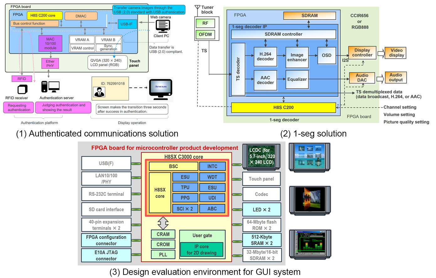
Since around 2008, in cooperation with multiple companies, Renesas started to create solutions (examples are shown in Figure 2) and develop demos, in combination with the respective technologies and IPs owned by such companies, as well as developing the evaluation environment.
(1) Authenticated communications solution
Various kinds of solutions can be structured in this way, such as this authentication platform obtained by integrating the H8S C200 core IP, an Ethernet MAC, DMAC, USB interface, touch-panel control, and RFID control in a single chip (FPGA).
(2) 1-seg solution
1-seg is a lower-bandwidth digital television standard mainly used in Japan and Brazil. In this solution, a 1-seg decoder IP in which 1-seg processing proceeds with the use of logic circuits, and the H8S C200 core IP, miniaturization of the system and high-quality output pictures are obtained.
(3) Design evaluation environment for GUI system
By integrating the H8S C200 core IP and a 2D drawing function IP core required as part of handling a GUI in an FPGA, higher drawing performance than would be achieved by software processing on its own can be realized, and the design of a GUI system can be evaluated. Note that in this solution, the H8SX C3000 core IP was finally selected for use as the core.
In these ways, the H8S C200 core IP can easily be implemented in FPGAs. As the core is small, it provides an easy way of incorporating microcontroller functions in FPGAs, leading to the realization of various kinds of solutions spanning a wide variety of control applications.
FPGA Microcontroller
As a result of these activities, Macnica, Inc. also released an H8S C200 core IP in 2014. The core is for implementation on an Intel® MAX® 10 that incorporates A/D converters.
The H8S C200 core IP is a soft macro that includes standard microcontroller functions. On the other hand, until the release of the Intel MAX 10, FPGAs had not incorporated hard macros such as A/D converters that are included in general-purpose microcontrollers.
Renesas therefore decided to add a register interface for control of the incorporated A/D converters in the MAX 10 by the IP. The configuration of the registers was the same as that for the A/D converters in existing H8 and H8S microcontrollers. This enables users to operate the FPGA’s A/D converters in the same way as in the microcontrollers, eliminating the need for changes to existing software. To supplement the H8S C200 core IP, Renesas also prepared functions such as timers, an SCI, and I/O port circuits, equivalent to the functions of an H8 microcontroller, the H8/327. The IP thus born was the first true “FPGA microcontroller”. Furthermore, since the MAX 10 evaluation board as a development kit has an onboard D/A converter, Renesas made the D/A converter controllable through register interfaces common and made the D/A converter of the evaluation board operate in the same way as those of existing microcontrollers, leading to preparation of the function IP of the H8/3048 to form the second FPGA microcontroller.
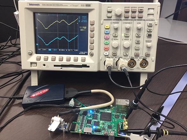
Figure 3 shows the evaluation environment for analog I/O described above. A commercial MAX 10 evaluation board and the software development environment for Renesas H8S microcontrollers (See the "Evaluation Environment for the FPGA Microcontroller" below) were used. As stated, in the evaluation project above, we implemented an FPGA microcontroller with the function IP of the H8/3048 in a MAX 10. When we input an analog signal from the onboard potentiometer, the H8S microcontroller detects the signal through an A/D converter of the MAX 10 and then outputs the signal value through an onboard D/A converter. The software repeats reading from the ADDRC register and writing to the DADR0 register. We were able to confirm the correspondence of the analog input and output values to each other.
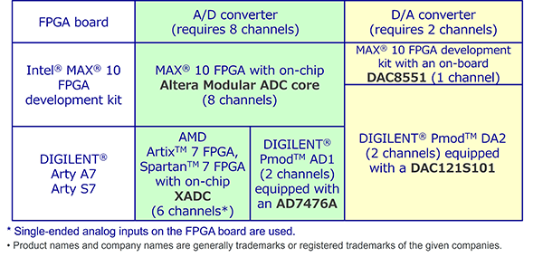
Table 1 lists the hard IP macros proven to work as A/D and D/A converters through evaluation to be usable in FPGAs, such as FPGAs with A/D converters including the MAX 10, and the A/D and D/A converters on FPGA boards.
We earlier described evaluation with the use of a MAX 10. We now introduce an example of implementing an FPGA microcontroller with the function IP of the H8S/2655 in an AMD (Xilinx) FPGA. This FPGA board consists of 1: an Arty A7 FPGA board and 2: a Pmod™ AD1 and a Pmod DA2, all manufactured by DIGILENT®. See Figure 4.
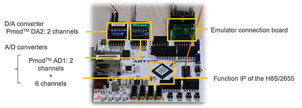
The FPGA board has a 6-channel A/D converter incorporated in the FPGA, a 2-channel A/D converter implemented with the use of a Pmod AD1, and a 2-channel D/A converter implemented with the use of a Pmod DA2. The function IP of the H8S/2655 includes control of the individual converters on the FPGA board.
Note that the emulator connection board is for connection to the software development environment described in the next section, "Evaluation Environment for the FPGA Microcontroller".
Evaluation Environment for the FPGA Microcontroller
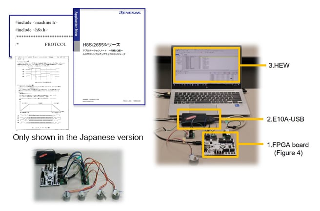
We now introduce the evaluation environment for the FPGA microcontroller created by using an FPGA board equipped with an FPGA microcontroller to implement the function IP of the H8S/2655. The environment is shown in the photograph on the right side of Figure 5. The environment consists of 1) the FPGA board, 2) an E10A-USB on-chip debugging emulator from Renesas, and 3) the High-performance Embedded Workshop (HEW) integrated development environment. Elements 2 and 3 are used for the development of the software for the H8S microcontroller. For connecting an FPGA board and an E10A-USB, jumper wires and connectors are used. In this evaluation, we used an emulator connection board manufactured by a partner company.
Here we used the sample program for an example of driving a 4-phase stepping motor in an application note for H8S/2655. With an FPGA microcontroller and a C-source sample program, we confirmed that the FPGA microcontroller with the function IP of the H8S/2655 was capable of controlling the stepping motor as well as an actual H8S/2655 microcontroller. The lower-left part of Figure 5 shows an example of the implementation of the FPGA microcontroller for controlling the 4-phase stepping motor.
This evaluation environment can also be used with the implementations of the function IPs of the H8/3048 and H8/327 described above.
The CPUs in H8, H8S, and H8SX microcontrollers (except for the H8/500) are object-level compatible, so they can be used in a common development environment, with the E10A-USB being used as the emulator.
Evolving FPGA Microcontrollers
With the miniaturization of fabrication processes, FPGAs have been improved in terms of higher speed, larger capacity, and richer ranges of functions, such as analog and interface functions, leading to greater usability.
FPGA microcontrollers have been well received by their actual users. Renesas therefore is strengthening the range of peripheral IPs of microcontrollers and increasing the number of variants implemented as FPGA microcontrollers in response to improvements in the speed and capacity of FPGAs.
The H8S core IP FPGA microcontroller described in this blog post is a successor to the H8S and H8 microcontrollers, on which users can reuse any application software they find useful. We hope that the most appropriate usage of devices for users, over a long and continuous period, can easily be realized with the aid of FPGA microcontrollers. Using not only general devices with fixed functions but also IP products enables taking advantage of the intellectual assets of microcontroller products, and extending and customizing functions, allowing the use of the most appropriate functions in the most appropriate format, beyond the usage of general devices. In addition, timely moves to the most appropriate devices in response to changes in the external environment are easy.
FPGA microcontrollers provide various benefits through the flexibility of FPGAs. For example, peripheral IPs can be added to FPGA microcontrollers, with expansion interfaces prepared. The following web pages describe examples of controlling motors with the use of this benefit.
In Conclusion
The FPGA microcontroller is a solution for continuous usage in various formats for a long period of time to take advantage of the usability of microcontrollers. We hope that users consider such solutions not only for original microcontrollers but also as a measure for handling operations at EOL. Visit our Microcontroller IPs for FPGA application page to learn more about FPGA microcontrollers.
As well as H8 and related processors, the processor IPs include the SH-2A, SH3-DSP, SH-4, SH-4A, RX, and M32R. We will be introducing FPGA applications for those processors in the future.
In addition, when you need to learn how to use IPs, Renesas can organize IP seminars to introduce brand-new information on IPs, solutions with the use of IPs, and so on. The seminars are held within the solution seminars in Renesas semiconductor seminars. We encourage your participation if you have an interest.
Thank you for reading through this post. For inquiries about Renesas IP products, please contact us at [email protected].