Ultra-Low Power Broadband 8- to 14-Bit Data Acquisition Kit
Quickly evaluate the amplifier, filter and analog-to-digital converter (ADC) signal chain's total performance in your application. Pairing with Renesas' ADC...

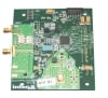
Renesas offers two options for evaluating high-speed analog-to-digital converter products with LVDS and/or LVCMOS outputs. A complete, turnkey evaluation platform is available, which includes data capture hardware and software to process and display acquired data. This system provides the fastest and easiest path to evaluating an ADC since no additional software coding is required of the user.
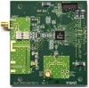
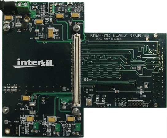
The second option is an adapter board that facilitates the connection of an ADC daughter card to an FMC-based FPGA development board. This solution offers greater flexibility since the user has full access to the FPGA functionality and can therefore perform signal processing operations and/or "hardware in the loop" simulations. No software is provided for this option since there are a wide variety of supported FGPA development boards.
More information on JESD204B high-speed serial outputs
| Attribute | Complete Evaluation Platform | FMC Motherboard |
|---|---|---|
| Motherboard | KMB-001LEVALZ: LVDS interface KMB001CEVAL: CMOS interface |
KMB-FMC-EVALZ |
| Motherboard contains FPGA | Yes | No |
| Capture Memory | 1 million words | Depends on FPGA development board |
| Uses ADC Daughter Card | Yes | Yes |
| Includes Konverter Analyzer for processing and displaying acquired data | Yes | No |
| Allows access to FPGA code | No | Yes |
| Allows for "hardware in the loop" simulations | No | Yes |
Disclaimer: THIS MATERIAL IS PROVIDED “AS-IS” FOR EVALUATION PURPOSES ONLY. RENESAS ELECTRONICS CORPORATION AND ITS SUBSIDIARIES (collectively, “Renesas”) DISCLAIM ALL WARRANTIES, INCLUDING WITHOUT LIMITATION, FITNESS FOR A PARTICULAR PURPOSE AND MERCHANTABILITY. Renesas provides evaluation platforms and design proposals to help our customers to develop products. However, factors beyond Renesas' control, including without limitation, component variations, temperature changes and PCB layout, could significantly affect the product performance. It is the user’s responsibility to verify the actual circuit performance.
|
|
|
|
|---|---|---|
| 类型 | 文档标题 | 日期 |
| 手册 - 开发工具 | PDF 2.02 MB | |
| 指南 | PDF 1.02 MB | |
| 手册 - 开发工具 | PDF 509 KB | |
| 手册 - 开发工具 | PDF 760 KB | |
| 指南 | PDF 715 KB | |
| 手册 - 开发工具 | PDF 503 KB | |
6 items
|
||
Quickly evaluate the amplifier, filter and analog-to-digital converter (ADC) signal chain's total performance in your application. Pairing with Renesas' ADC...
This ISLA214P50-55210EV1Z is an evaluation platform featuring Renesas' ultra-high, dynamic range, fully differential amplifier (FDA), the ISL55210, and the high-speed,...
简介 |
购买 / 样片 |
|
|---|---|---|
| 器件号 | ||
KMB-FMC-EVALZ 有效 可提供样片 |
FMC FPGA ADC Motherboard - 40MSPS to 500MSPS Operation | 获取样片, |
KMB-001LEVALZ 有效 可提供样片 |
LVDS Interface Motherboard for Use with Daughter Card | 获取样片, |
KMB-001CEVALZ 有效 可提供样片 |
CMOS Interface Motherboard for Use with Daughter Card | 获取样片, |
KDC5612EVAL 有效 可提供样片 |
KDC5612P Low Power, Dual-Channel 12-Bit ADC Daughter Card | 获取样片, |
KDC5514EVALZ 有效 可提供样片 |
KDC5514 Low Power, Dual-Channel 14-Bit ADC Daughter Card | 获取样片, |
KDC5514-Q48EVAL 有效 可提供样片 |
KAD5514P Low Power, Dual-Channel 14-Bit ADC Daughter Card - 48QFN Package | 获取样片, |
KDC5512HEVALZ 有效 可提供样片 |
KADC5512 High-Performance 12-Bit ADC Daughter Card | 获取样片, |
KDC5512HEVAL 有效 可提供样片 |
KADC5512 High-Performance 12-Bit ADC Daughter Card | 获取样片, |
KDC5512H-Q48EVAL 有效 可提供样片 |
KADC5512 High-Performance 12-Bit ADC Daughter Card - 48QFN Package | 获取样片, |
KDC5512-Q48EVAL 有效 可提供样片 |
KADC5512 High-Performance 12-Bit ADC Daughter Card - 48QFN Package | 获取样片, |
ISLA224S25IR48EV1Z 有效 可提供样片 |
ISLA224S Series Dual-Channel 14-Bit 250MSPS Evaluation Board - 48LD QFN Package | 获取样片, |
ISLA224IR72EV1Z 有效 可提供样片 |
ISLA224IR72 Dual-Channel 14-Bit 250MSPS ADC Evaluation Board - 72QFN Package | 获取样片, |
ISLA216S25IR48EV1Z 有效 可提供样片 |
ISLA216S Series 14-Bit 250MSPS Evaluation Board - 48LD QFN Package | 获取样片, |
ISLA216IR72EV1Z 有效 可提供样片 |
ISLA216IR72 Single 16-Bit 250MSPS Evaluation Board - 72LD QFN Package | 获取样片, |
ISLA214S50IR48EV1Z 有效 可提供样片 |
ISLA214S50 Series 14-Bit 500MSPS Evaluation Board - 48LD QFN Package | 获取样片, |
ISLA214P50IR72EV1Z 有效 可提供样片 |
ISLA214P50IR72 Single 14-Bit 500MSPS Evaluation Board - 72LD QFN Package | 获取样片, |
ISLA214P50-55210EV1Z 有效 可提供样片 |
ISL55210, ISLA214P50 Series 14-Bit 500MSPS Evaluation Board - 72LD/16LD TQFN Packages | 获取样片, |
ISLA214IR72EV1Z 有效 可提供样片 |
ISLA214IR72 Single 14-Bit 250MSPS Evaluation Board - 72LD QFN Package | 获取样片, |
ISLA118P50IR72EV1Z 有效 可提供样片 |
ISLA118P50 Series I2E 8-Bit 500MSPS Daughter Card - 72LD QFN Package | 获取样片, |
ISLA112P50IR72EV1Z 有效 可提供样片 |
ISLA112P50 FemtoCharge™ I2E 12-Bit 500MSPS Daughter Card - 72LD QFN Package | 获取样片, |
ISLA112P50/55210EV1Z 有效 可提供样片 |
PCB for ISLA112P50 ADC with an ISL55210 Amplifier Drive, BPF - 72LD QFN Package | 获取样片, |
ISLA110P50IR72EV1Z 有效 可提供样片 |
ISLA110P50 FemtoCharge™ I2E 10-Bit 500MSPS Daughter Card - 72LD QFN Package | 获取样片, |

The high-speed ADC evaluation platform enables rapid testing and performance validation of the entire portfolio of low-power 8 to 16-bit, 40 to 500MSPS high performance analog-to-digital converters.
Good morning. My name is Michael Steffes, Applications Manager in the High-Speed Amplifier area. This morning, we're demonstrating a new evaluation platform including our high-speed amplifier, the ISL55210 and our 12-bit 500 Mega-Sample ADC.
From Intersil, you would require a motherboard which allows you to test many different kinds of converters. This is available online. On that, we attached two different daughter boards. Normally, we deliver a converter daughter boards with only two transformers. This requires a 10dBm board edge power level but works just fine. What we're demonstrating this morning is a new daughter board which includes an amplifier stage which reduces the board edge power to -10dBm, much more realistic for systems.
So once you get a motherboard, you would download the software which is the converter software - it's a free download - to drive the motherboard through a USB connection and be able to attach on any of the series of daughter boards including the amplifier or different converters.
So go online today and look for each of these elements for your high-performance converter data acquisition needs.