
Low Voltage Driver for Synchronous Rectification Evaluation Board
跳转至页面部分:
概览
简介
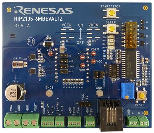
The HIP2105-6MBEVAL1Z is an evaluation tool for the HIP2105 and HIP2106A half bridge MOSFET drivers. This tool consists of a motherboard and HIP2105DBEVAL1Z or HIP2106ADBEVAL1Z evaluation daughter cards. The motherboard platform provides an on board microcontroller that is used to generate appropriate control inputs to the HIP2105 or HIP2106A. The frequency, the PWM duty cycle, and the dead time provided by the microcontroller are user adjustable.
For customers who want to provide their own external signals, the on board controller can be configured to allow the daughter cards to be controlled by externally provided inputs.
The daughter cards can also be used as stand-alone units mounted on a customer-designed main board that incorporates customer-selected bridge FETs and any other external circuits desired. The daughter cards have optional circuits so that the HIP2105 or HIP2106A can be configured as required by the customer's application.
特性
- Adaptive shoot-through protection, HIP2106A only
- HI/PWM and LI inputs, HIP2105 only
- 0.4Ω ON-resistance and 4A sink current capability
- Low tri-state hold-off time (20ns), HIP2106A only after 20ns
- Supports 3.3V and 5V HI/LI or PWM input
- Power-On Reset (POR)
应用
应用
- Wireless chargers
- High frequency low profile high-efficiency DC/DC converters
- High current low voltage DC/DC converters
- E-cigarettes
Processing table
HIP2105-6MBEVAL1Z 过时 |

Tips for Using This Parametric Table:
- Hide Filters button in header: Collapse or expands filters
- Column sort buttons in header: Sort Column alphabetically / numerically descending or ascending
- Reset button in header: Reset all filters to the page default
- Full Screen button in header: Expand the table to full screen view (user must close out of full screen before they can interact with rest of page)
- Export button in header: Export the filtered results of the table to an Excel document
- Filter parts search bar in header: Type to filter table results by part number
- Hide column button in column headers: Select to hide columns in table
- AND / OR toggle switches in header: Toggles the logic of this particular filter to be “AND” or “OR” logic for filtering results
- Multiselect checkboxes at beginning of each row in table: Select these checkboxes to compare products against each other
- Document icon next to product name in row: View the featured document for this product
- Chip icon next to the right of the document icon in row: View the block diagram for this product
- Cart icon to the right of the chip icon: Indicates that samples are available for this product
视频和培训
Power 101 Webinar
Intersil’s introductory course on power electronics discussing the basic building blocks of a DC-DC power system: linear and switching regulators.
Transcript
Power 101 - Introduction to Intersil Power Products
Welcome to Intersil’s introductory course on power electronics. This presentation discusses the basic building blocks of a DC/DC power system.
DC/DC Converter Choices for a Designer
In power management there are two choices that the designer has regarding his DC/DC design: a switcher or a linear regulator.
Linear or low dropout regulators are non-switching devices that take the output voltage to a level lower than the input. The way they do this function yields lower efficiency and can generate more heat than a switcher at the same power level. The distinct advantages for linear regulators are they are easy to use and they don’t generate any switching noise in the system. Linear regulators are ideal in low output current applications typically in the 1A to 2A or less range because they don’t require many external components and therefore are typically more cost effective as well at the low current levels.
Switching regulators have more external parts and need more attention to design, but are flexible for a wide range of power levels. Other benefits include higher efficiency, lower power dissipation and therefore better thermal performance. One of the biggest concerns with switching regulators is that they can generate switching noise that could show up throughout the system.
Linear Regulators
A linear regulator is essentially made up of three components: the pass element, the error amplifier and the reference.
Of these components, the pass element is the one that most influences the device’s key specifications. The output of the error amp adjusts the resistance of the pass element in order to create the correct voltage change for a given output current.
There are a number of possible choices for the pass element, each with its own advantages and disadvantages.
Three Linear Regulators
Here we discuss three different types of linear regulators. The first category is general purpose linear regulators. They use transistors as the pass element, such as an NPN, which is very inexpensive and has a low output impedance but suffers from many disadvantages compared to modern LDOs. The most obvious disadvantage is the large dropout voltage – the minimum difference in voltage between the input and the output.
The second type of linear regulator uses a power MOSFET as a pass element to offer much smaller dropout voltage. However, it does not have other modern features and has minimal protection circuitry.
Finally, high performance LDOs use P-CH MOSFETs as pass elements to offer the best dropout voltage and they offer additional performance and protection features.
Intersil LDO Family
Intersil LDOs span the spectrum between the second and third type of linear regulators. They provide a range of feature sets while maintaining a competitive cost model.
Both single supply and split power supply LDOs are available for critical applications. The supported VIN range is from 1V to 40V and output current is from 0.05A to 3A.
We have a broad portfolio of LDOs.
Switching DC/DC Converters
Now we will examine the switching regulators.
Switching Basics
An ideal switching regulator uses the properties of inductors and capacitors, along with a switch and either a second switch or diode, to transfer energy from one potential to another with no losses. The inductor stores energy from the input in its magnetic field and discharges the energy into the output, varying with the state of the switch. Meanwhile, the capacitors maintain a constant voltage.
Non-ideal inductors, capacitors and switches do create losses; however, the switching regulator is still able to maintain a high efficiency over a wide range of operation. An important result of the non-ideal behavior of the circuit components and the constant on and off of the switches is the introduction of ripple currents in the input and output capacitors that turn into voltage ripple and noise, and electromagnetic noise from parasitic inductance in the board and the inductor itself.
Key Power Management Terms to Remember
Here are the three choices in selecting the proper type of converter in the DC/DC design.
A buck converter steps down the input voltage to a LOWER level at the output. An example would be a 5V input to a 3.3V output or a 12V input to a 1.2V output.
A boost converter does the opposite function of a BUCK converter. It steps UP the input voltage to a higher level at the output. For example, taking a 3.3 input voltage to 12V or 3.3V to 5V.
A buck-boost converter is capable of bucking or boosting the input voltage depending on what the output is set to and what the input voltage actually is. This function is mainly used in battery applications where for example you could start with a fully charged battery with an input voltage of 4.2V and the output set to 3.3V. The converter would step down or BUCK the input voltage to the 3.3V level, but if the load continues to draw power from the battery while it is not being charged any more, the input voltage would then get lower over time. Once the battery drains down below 3.3V, the converter would then boost the output to 3.3V. It would stay in this mode until the battery charger is plugged back in and the battery voltage increases to a predetermined level higher than the output. At that point the device switches back to BUCK mode again.
In general, most of the designs you will talk about with designers will be a BUCK type controller which means the input voltage will be higher than the output voltage.
Basics: Synchronous Buck Converter Operation
Let’s discuss the basics of a synchronous buck converter. First, the term “buck regulator,” also known as a step-down regulator, indicates that you are stepping down or bucking the input voltage to a lower DC voltage. The term synchronous buck indicates that a MOSFET is used as a lower switch (versus a standard buck regulator that would have a Schottky diode as a lower switch). The main benefit of a synchronous buck regulator versus a standard buck regulator is better efficiency due to a lower voltage drop of the MOSFET vs. a diode.
Looking at the block diagram on the right, we see a PWM controller which generates the timing information for the lower and upper MOSFETs. We also see at the output, a feedback connection to the controller. This is used to regulate the output in case the output voltage changes due to load changes.
Let’s now look at the phase voltage. The phase voltage is generated from the PWM regulator turning on the upper and lower MOSFETs. TON as you can see on the phase voltage graph is the upper MOSFET turning on, TOFF is the upper MOSFET turning off. Duty cycle is a term used to describe the relationship of TON over TON plus TOFF.
The output voltage of a synchronous buck controller is a function of the input voltage times this duty cycle. Also on this slide, we are looking at the charging and discharging of the output inductor, along with the current in the upper and lower MOSFETs.
Basics: Synchronous Boost Converter Operation
A synchronous boost regulator, also known as a step up regulator, uses the same components as the buck regulator, but in reverse order. The input voltage is connected directly to the inductor and the output and common ground are switched on and off with the MOSFETs. While the calculation for the duty cycle remains the same, the change in component order results in a new calculation for VOUT where it is equal to VIN times the reciprocal of one minus the duty cycle.
Looking at the phase voltage graph, this time it is the lower MOSFET that is being turned on and off and it is the upper MOSFET that can be replaced with a diode for a standard configuration.
Basics: Buck-Boost Converter Operation
There is more than one way to make a buck-boost circuit, but the most common one simply places buck circuitry in series with the boost circuitry. By controlling which switches are held open, closed or actively switching, either the buck or the boost function is enabled.
Device Options for a Switching Converter
Switching regulators include most of the components required for the design, including the switch mode FET. However, the integrated FETs limit the maximum current that can pass through the system. Most switching regulators operate in the region of 1A to 6A.
For higher output currents, a switching controller is used. It drives external FETs, allowing the user to select parts that can handle much higher currents. The down side to this is a more complex design that takes up more space. Some controllers do not drive the FETs directly and require an external driver as well. External drivers and drivers integrated with MOSFETs (called DrMOS) are in the Intersil portfolio as well.
The most highly integrated devices offered are power modules. They include almost all components and have a very high power density, allowing them to source as much current as most controller designs.
Over the next few slides we will look at some of the available devices from Intersil.
Single Output Switching Regulator Product Portfolio
Here are several devices from Intersil’s large portfolio of switching regulators. Input voltage ranges can go up as high as 60V and output current up to 8A.
Multi-Output Switching Regulator Product Portfolio
There are also a number of regulators with multiple outputs, including a mix of switching regulators and LDOs.
Switching Buck Controllers
Here is a quick table of Intersil’s analog controller products in different categories. This is just a sample of products available in each product category. Note the much higher output currents available.
Analog Power Modules
Finally, Intersil’s analog power module product offering includes a broad line of products for almost any application, whether it be a single 4A all the way to modules operating at 240A in parallel.
Additional Resources
A full list of products can be found on our website. Also, the PowerCompass tool will provide you with parts matching your design specifications.
Summary
In summary, the two choices for DC/DC power management are linear regulators and switching regulators. Linear regulators have lower noise and are easy to design at the cost of efficiency, while switching regulators have great versatility and efficiency, but produce a lot of noise. Intersil has a large portfolio of these devices with varying levels of integration to fit the many possible applications.
Video List