

Radar Transceivers: Key Components for ADAS & Autonomous Driving
- Blog 1: Why Do We Need Radar?
- Blog 2: Basics of FMCW Radar
- Blog 3: Radar Range: How Far Can a Radar "See"?
- Blog 4: Radar Resolution: How Accurate Can a Radar Be?
- Blog 5: Radar Architecture: How to Connect Different Radar Sensors
- Blog 6: How to connect the antennas?
- Blog 7: Antennas for Automotive Radar
1. mmWave MMIC to antenna interfaces
In the previous issue of Renesas’s radar blog, we discussed different antenna options for transmitting and receiving the radar signal. Now we will focus on how to connect a monolithic microwave integrated circuit (MMIC) radar transceiver to the antennas in a way that guarantees an efficient transfer of the signals. At millimeter-wave (mmWave) frequencies, any transitions between two different transmission lines, on the chip, board, or antenna, can have a significant impact on the performance of the overall system. Any degradation or malfunction in the interfaces will cause signal loss or interference, leading to reduced performance or system failures. Therefore, one of the key challenges in the design of a radar module will be maintaining high signal integrity and low losses throughout the entire RF signal path between the MMIC and the selected antennas.
2. Chip to board BGA interface
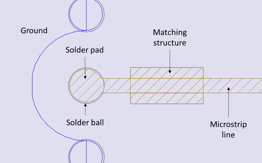
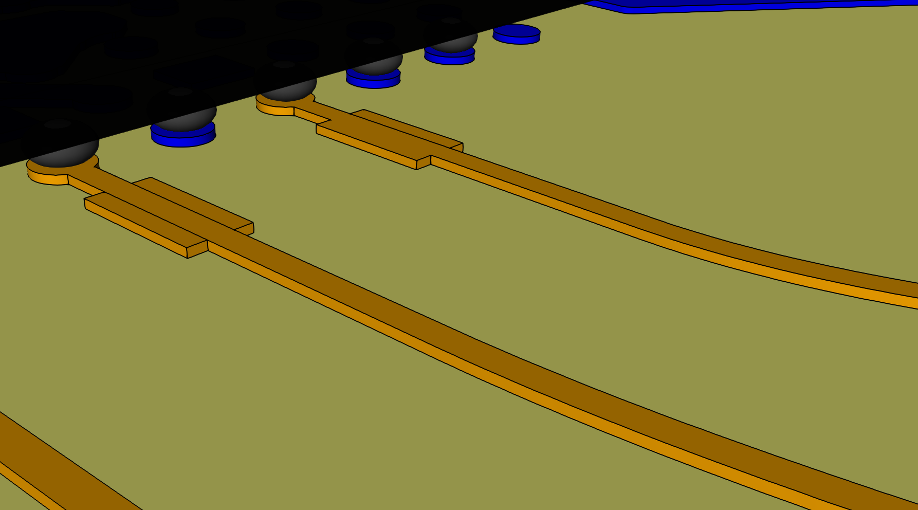
t millimeter wave frequencies, chip-to-board transitions are challenging due to the short wavelengths involved. The most common approach is using the BGA to transfer the RF signals from the chip to a transmission line printed on the board, usually microstrip lines, but also striplines, coplanar waveguides (CPW) or substrate integrated waveguides (SIW) could be used. This allows a direct connection to on-board antennas, such as patch arrays.
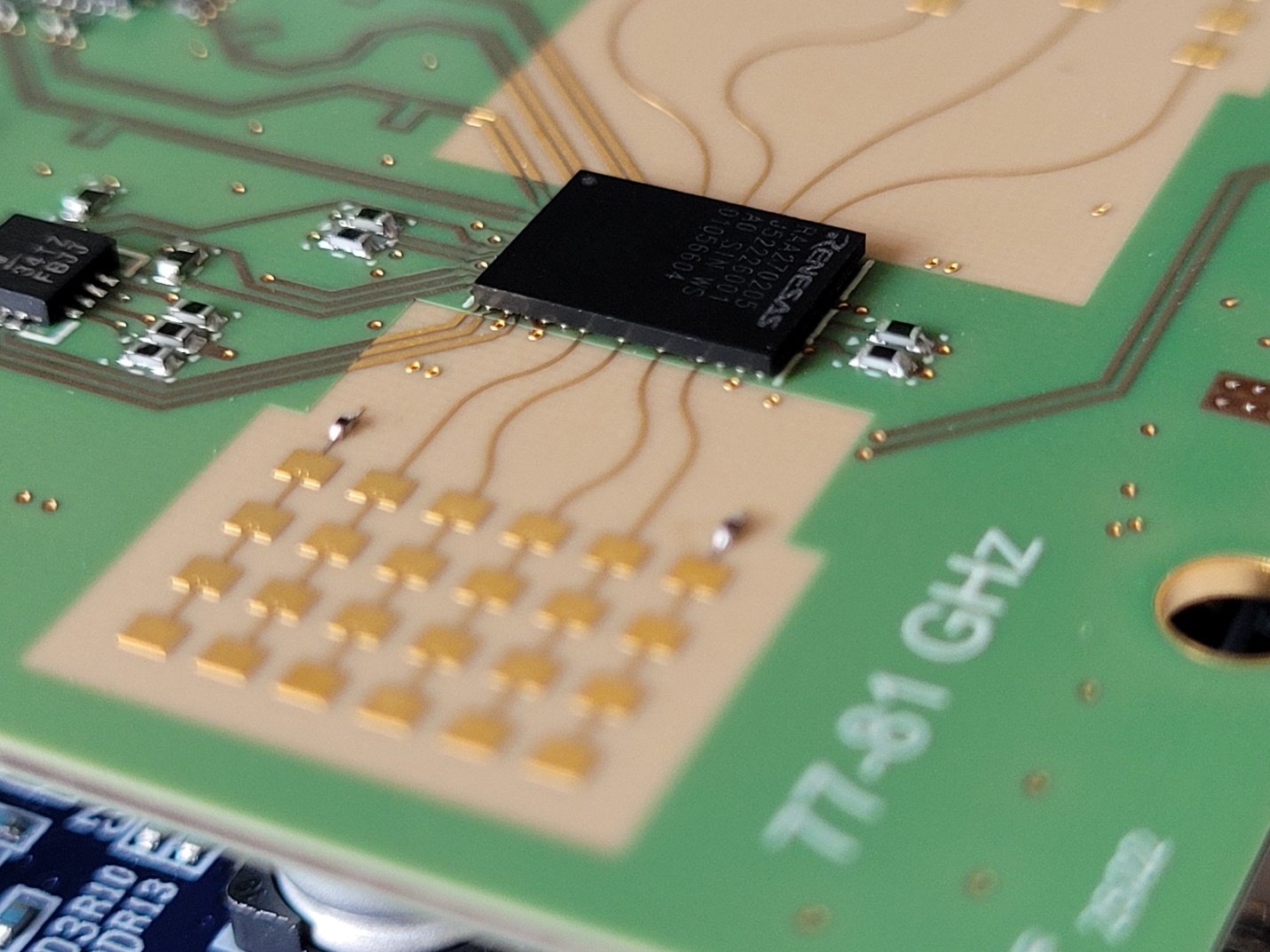
The transition structure needs to be designed to match the impedance of the MMIC to that of the transmission line on the board, to minimize losses and reflections. This is critical for efficient power transfer and optimal radiation efficiency and can be achieved by tapering the width of the line and/or adding matching structures.
A careful design of the interface can help minimize the effect of crosstalk and interference, which can be significant at mmWave frequencies. It is also important to ensure good connection with the PCB ground, to further reduce interference and improve the signal-to-noise ratio.
High-quality, low-loss materials should be used for manufacturing the board, to reduce the losses on the transmission lines between the chip and the antenna. Additionally, special care must be taken during the assembly process, to ensure a proper alignment between the soldering balls and the lines, to avoid mismatching and minimize the parasitic effects.
Here again, use of electromagnetic simulation tools is capital to optimize the interface. The design must be adapted for the desired stackup and PCB layout, to guarantee the targeted performance is achieved. The simulation can be extended to include the antennas and, in the end, the whole PCB, and analyze the effects of material and manufacturing tolerances.
3. Launcher on board for waveguide antennas
When 3D waveguide antennas are used, it is necessary to add a second transition, from the board to the antenna module. For that, the transmission line modes that carry the signal on the PCB (e.g. the microstrip quasi-TEM modes) have to be converted to waveguide modes.
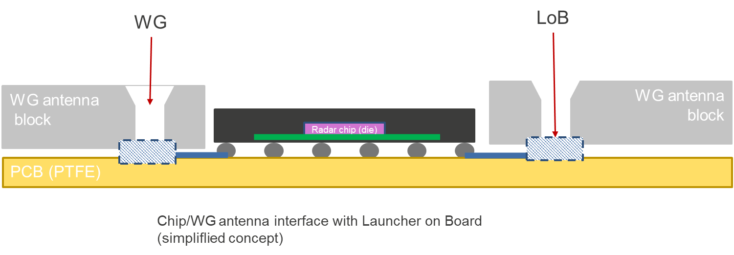
A waveguide launcher on board (LoB) is a small interface designed at the end of the PCB transmission line, which will provide a means for the electromagnetic waves generated by the radar MMIC to be coupled into the waveguide antenna. This can be a printed element (probe) or an aperture in a conducting plane.
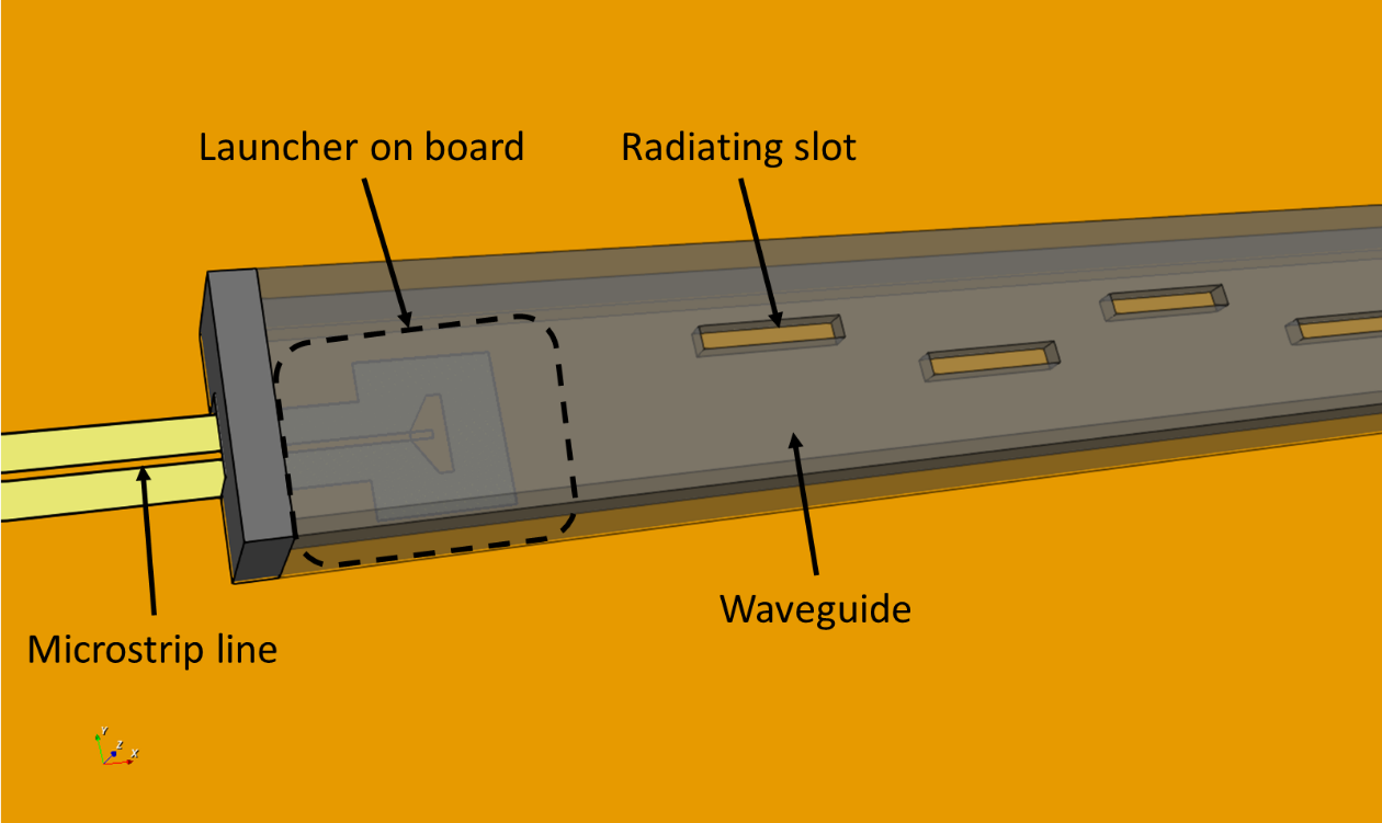
The shape of the launcher on board must be optimized to maximize the coupling efficiency and to match the impedance of the transmission line on the board to the impedance of the waveguide. To ensure a smooth transition, tapered shapes are normally used. Indeed, sharp edges and abrupt discontinuities would cause high reflection levels, leading to power loss and signal distortion.
The size of the waveguide launcher is also of capital importance. It needs to be small enough to fit on the board, keeping the line lengths as short as possible. On the other hand, the laws of physics require that it be large enough to efficiently couple the signal from the PCB transmission line to the waveguide antenna. Here again, electromagnetic simulation tools are unavoidable to optimize the design of the launcher and accurately predict its performance.
High precision manufacturing and assembly will be required, to guarantee accurate contact and alignment between the board and the waveguide antenna. Any tolerances in the alignment or air gaps may lead to high loss of performance.
4. Launcher on package for waveguides antennas
With a waveguide launcher on package, the mmWave signals still need to be routed on the PCB. That means that high quality, low-loss materials are required. This could be avoided with a direct coupling between the radar transceiver and the 3D antennas using a waveguide launcher in package (LiP), also known as Launcher on Package (LoP). The LiP/LoP is used to interface the MMIC with an external waveguide that feeds the antenna. It can be integrated into the package of the MMIC, avoiding the need for routing on the PCB, so that now lower-cost substrate materials can be used.
The package of the MMIC must be designed to accommodate a waveguide launcher for each transmit and for each receive channel of the radar transceiver. There are two options to implement the launcher in package: top- or bottom-launch.
In a top-launch configuration, the antenna is placed on top of the package, and will require mechanical support to guarantee the alignment and stability. The RF signals will be coupled to the waveguide without having to use any balls of the BGA.
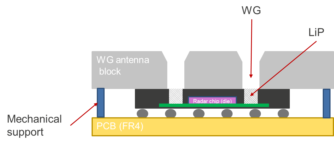
With the bottom-launch approach, the MMIC and the antennas are placed on opposite sides of the PCB. Some ball of the MMIC’s ball grid array (BGA) will be used to define the waveguide transition. The mmWave signals will be couples to the antenna by through a short waveguide defined by the BGA and plated wholes on the PCB.

In both cases, each launcher has a minimum size, dictated by the operating frequency, the overall size of the package will be increased with respect to that of the conventional BGA interfaces.
As in the case of the launcher on board, the launcher in package needs to be designed to provide a smooth transition from the MMIC to the waveguide, minimizing the losses due to reflections and scattering, while matching the impedance of the chip to that of the waveguide.
The feeding network in the redistribution layers of the MMIC must be designed to provide a uniform distribution of power to each waveguide launcher, while minimizing the coupling between the different RF ports. Also, the materials used in the packaging need to be carefully chosen, as they can affect the performance of the waveguide launcher.
The mechanical stability of the package with LiP is important for ensuring long-term reliability. The structure should be designed to withstand mechanical stresses and temperature variations. Also, it is capital to ensure the accurate alignment and proper contact between the launcher and the waveguide, to avoid not only loss of performance due to mismatch, but also to reduce the leakage which would cause increased coupling between the different RF channels.