| Pitch (mm) | 1.27 |
| Lead Count (#) | 8 |
| Pkg. Dimensions (mm) | 4.9 x 3.9 x 1.5 |
| Pkg. Code | MSA |
| Pkg. Type | SOICN |
| Moisture Sensitivity Level (MSL) | 1 |
| Pb (Lead) Free | Yes |
| ECCN (US) | EAR99 |
| HTS (US) | 8542330001 |
| RoHS (ICL7621DCBAZ-T) | Download |
| Lead Count (#) | 8 |
| Carrier Type | Reel |
| Moisture Sensitivity Level (MSL) | 1 |
| Pitch (mm) | 1.3 |
| Pkg. Dimensions (mm) | 4.9 x 3.9 x 0.00 |
| Pb (Lead) Free | Yes |
| Pb Free Category | Pb-Free 100% Matte Tin Plate w/Anneal-e3 |
| Temp. Range | 0 to +70°C |
| Country of Assembly | China |
| Country of Wafer Fabrication | United States |
| AVOL (dB) | 102 |
| Bandwidth (MHz) | 0.48 |
| CMRR (dB) | 91 |
| Channels (#) | 2 |
| Enable | No |
| Gain Min | 1 |
| IBIAS (nA) | 0.001 |
| IOUT (A) | 0.001 |
| IS per Amp (mA) | 0.1 |
| Length (mm) | 4.9 |
| MOQ | 2500 |
| Noise VN (nV/√Hz) | 100 |
| Offset Voltage (Max) (mV) | 4 |
| PSRR (db) | 86 |
| Pkg. Type | SOICN |
| Qualification Level | Standard |
| Rail-to-Rail Input | No |
| Rail-to-Rail Output | No |
| Single Supply Voltage Range (V) | 2 - 16 |
| Slew Rate (V/µs) | 0.16 |
| Thermal Shutdown | No |
| Thickness (mm) | 0.00 |
| VOUT (V) | 9.8 |
| VS (Max) (V) | 16 |
| VS (Min) (V) | 2 |
| Width (mm) | 3.9 |
| field__slew_rate_typical_ | 0.16 |
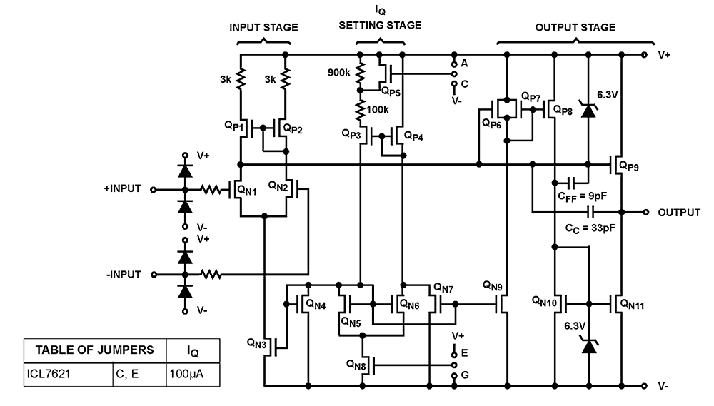
The ICL761X/762X series is a family of monolithic CMOS operational amplifiers. These devices provide the designer with high performance operation at low supply voltages and selectable quiescent currents. They are an ideal design tool when ultra low input current and low power dissipation are desired. The basic amplifier will operate at supply voltages ranging from ±1V to ±8V, and may be operated from a single Lithium cell. The output swing ranges to within a few millivolts of the supply voltages. The quiescent supply current of these amplifiers is set to 100µA at the factory. This results in power consumption as low as 200µW per amplifier. Of particular significance is the extremely low (1pA) input current, input noise current of 0. 01pA/√ Hz, and 1012Ω input impedance. These features optimize performance in very high source impedance applications. The inputs are internally protected. Outputs are fully protected against short circuits to ground or to either supply. Because of the low power dissipation, junction temperature rise and drift are quite low. Applications utilizing these features may include stable instruments, extended life designs, or high density packages.