Features
- Eight 0.7V HCSL differential output pairs
- Phase jitter: PCIe Gen3 < 1ps rms
- Phase jitter: PCIe Gen2 < 3.1ps rms
- Phase jitter: PCIe Gen1 < 86ps peak-to-peak
- Supports Zero Delay Buffer mode and Fanout mode
- Bandwidth programming available
- 3 selectable SMBus Addresses
- 50MHz to 110MHz operation in PLL mode
- 5MHz to 166MHz operation in Bypass mode
Description
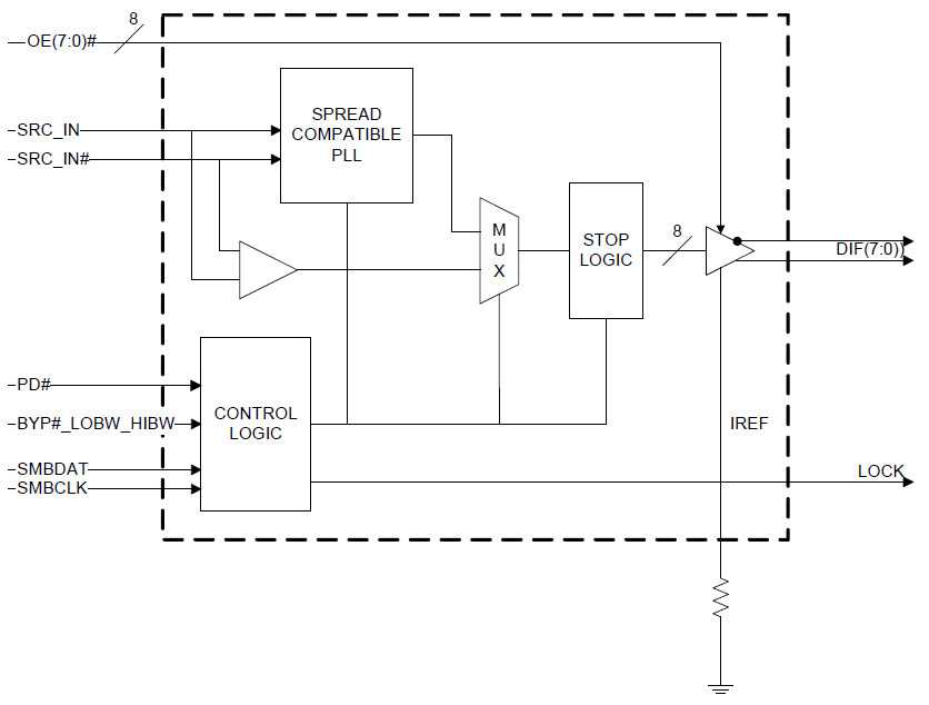
The 9DB833 zero delay buffer (ZDB) supports PCIe Gen3 requirements while being backward compatible with PCIe Gen2 and Gen1. The 9DB833 is driven by a differential SRC output pair from a 932S421 or 932SQ420 or equivalent main clock generator.
Parameters
| Attributes | Value |
|---|---|
| Temp. Range (°C) | -40 to 85°C, 0 to 70°C |
Package Options
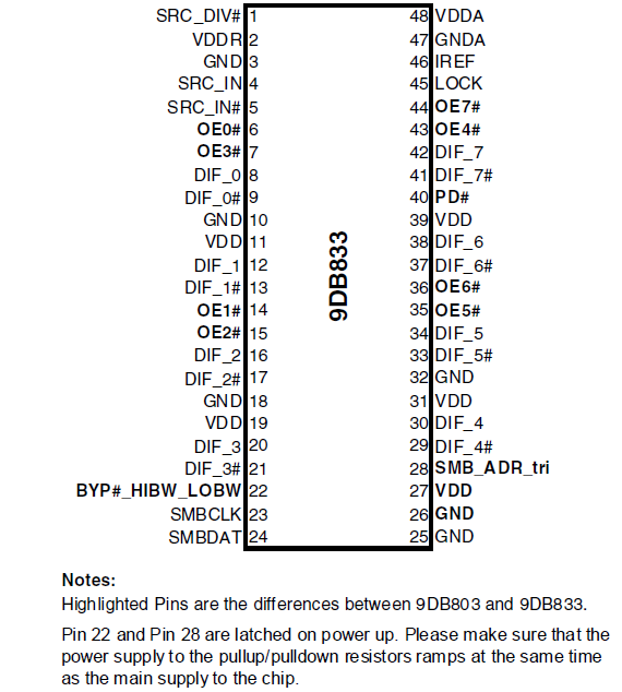
| Pkg. Type | Pkg. Dimensions (mm) | Lead Count (#) | Pitch (mm) |
|---|---|---|---|
| TSSOP | 12.5 x 6.1 x 1.0 | 48 | 0.5 |
Applied Filters:
Filters
Software & Tools
Sample Code
Simulation Models
This is the first video in our PCIe series. In this video, we define PCIe architectures, focusing on common and separate clock architectures. Watch the rest of the video series below where Ron will cover the impact of different timing architectures.
In this episode, Ron Wade from IDT (acquired by Renesas) explains PCIe common clocking and its impact on timing solutions. Learn about using a single clock source, fan-out buffers, and the considerations for spread spectrum and non-spread spectrum clocking in PCIe systems.
In this video, we explore PCIe with separate reference clocks and the effects of clock selection. Learn how separate reference clocks work and their impact on system performance and stability.
This video provides a high-level overview of Separate Reference Clock with Independent Spread (SRIS) architectures for PCI Express systems, additional performance requirements that this clocking architecture imposes on the reference clocks, and some system implications encountered trying to implement the architecture.
IDT (acquired by Renesas) engineer provides a brief tutorial on why zero delay buffers (ZDBs) are offered with two different bandwidths (1 MHz and 3 MHz). The reason has to do with jitter peaking when cascading PLLs.
Presented by Ron Wade, PCI Express timing expert.
Related Resources