
| CAD Model: | View CAD Model |
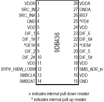
| Pkg. Type: | TSSOP |
| Pkg. Code: | PGG28 |
| Lead Count (#): | 28 |
| Pkg. Dimensions (mm): | 9.7 x 4.4 x 1.0 |
| Pitch (mm): | 0.65 |
| Moisture Sensitivity Level (MSL) | 1 |
| Pb (Lead) Free | Yes |
| ECCN (US) | EAR99 |
| HTS (US) | 8542.39.0090 |
| Lead Count (#) | 28 |
| Carrier Type | Reel |
| Moisture Sensitivity Level (MSL) | 1 |
| Qty. per Reel (#) | 2000 |
| Qty. per Carrier (#) | 0 |
| Pb (Lead) Free | Yes |
| Pb Free Category | e3 Sn |
| Temp. Range (°C) | -40 to 85°C |
| Accepts Spread Spec Input | Yes |
| Advanced Features | Safe Power Sequencing |
| App Jitter Compliance | PCIe Gen1, PCIe Gen2, PCIe Gen3, PCIe Gen4 |
| Architecture | Common, SRIS |
| C-C Jitter Max P-P (ps) | 50 |
| C-C Jitter Typ P-P (ps) | 25 |
| Chipset Name | Blackford, Clarksboro, Greencreek, Lindenhurst, Twincastle, San Clemente, Seaburg, Tylersburg |
| Clock Spec. | DB400 Gen3 |
| Core Voltage (V) | 3.3 |
| Diff. Input Signaling | HCSL |
| Diff. Inputs | 1 |
| Diff. Output Signaling | HCSL |
| Diff. Outputs | 4 |
| Diff. Termination Resistors | 16 |
| Feedback Input | No |
| Function | Zero Delay Buffer |
| Input Freq (MHz) | 50 - 100 |
| Input Type | HCSL |
| Inputs (#) | 1 |
| Length (mm) | 9.7 |
| MOQ | 2000 |
| Multiplication Value | 1 |
| Output Banks (#) | 1 |
| Output Freq Range (MHz) | 5 - 166.66 |
| Output Impedance | 85, 100 |
| Output Skew (ps) | 50 |
| Output Type | HCSL |
| Output Voltage (V) | 0.8 |
| Outputs (#) | 4 |
| PLL | Yes |
| Package Area (mm²) | 42.7 |
| Pitch (mm) | 0.65 |
| Pkg. Dimensions (mm) | 9.7 x 4.4 x 1.0 |
| Pkg. Type | TSSOP |
| Platform Name | Bensley, Caneland, Glidewell, Lindenhurst, Truland, Stoakley, Thurley, Cranberry Lake |
| Power Consumption Typ (mW) | 257 |
| Prog. Clock | No |
| Published | No |
| Reel Size (in) | 13 |
| Requires Terms and Conditions | Does not require acceptance of Terms and Conditions |
| Supply Voltage (V) | 3.3 - 3.3 |
| Tape & Reel | Yes |
| Thickness (mm) | 1 |
| Width (mm) | 4.4 |
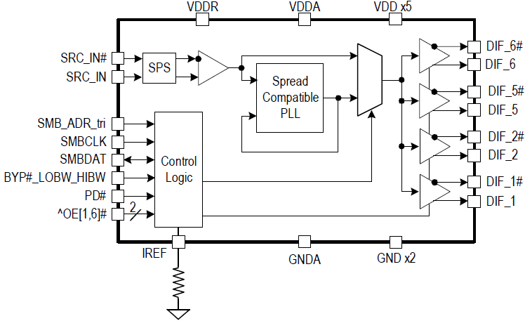
The 9DB436 is a zero delay/fanout buffer for PCI Express™ clocking. It supports PCIe Gen 1–3 in zero delay mode and PCIe Gen 1–4 in fanout mode. The 9DB436 also features a Safe Power Sequence (SPS) clock input. The 9DB436 is a pin-compatible upgrade to the 9DB433 and 9DB434.