
概览
简介
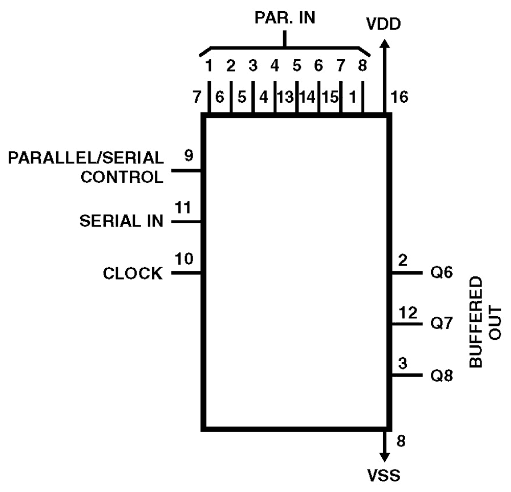
CD4014BMS - synchronous parallel or serial input/serial output CD4021BMS - asynchronous parallel input or synchronous serial input/serial output CD4014BMS and CD4021BMS series types are 8-stage parallel or serial input/serial output registers having common CLOCK and PARALLEL/SERIAL CONTROL inputs, a single SERIAL data input, and individual parallel JAM inputs to each register stage. Each register stage is a D-type, master-slave flip-flop. In addition to an output from stage 8, Q outputs are also available from stages 6 and 7. Parallel as well as serial entry is made into the register synchronously with the positive clock line transition in the CD4014BMS. In the CD4021BMS serial entry is synchronous with the clock but parallel entry is asynchronous. In both types, entry is controlled by the PARALLEL/SERIAL CONTROL input. When the PARALLEL/SERIAL CONTROL input is low, data is serially shifted into the 8-stage register synchronously with the positive transition of the clock line. When the PARALLEL/ SERIAL CONTROL input is high, data is jammed into the 8-stage register via the parallel input lines and synchronous with the positive transition of the clock line. In the CD4021BMS, the CLOCK input of the internal stage is forced when an asynchronous parallel entry is made. Register expansion using multiple packages is permitted. The CD4014BMS and CD4021BMS are supplied in these 16-lead outline packages: Braze Seal DIP H4T Frit Seal DIP H1F Ceramic Flatpack H6W
特性
- High voltage types (20V rating)
- Medium speed operation 12MHz (Typ.) clock rate at VDD-VSS = 10V
- Fully static operation
- 8 master-slave flip-flops plus output buffering and control gating
- 100% tested for quiescent current at 20V
- Maximum input current of 1µA at 18V over full package temperature range; 100nA at 18V and +25 °C
- Noise margin (full package temperature range)
- 1V at VDD = 5V
- 2V at VDD = 10V
- 2.5V at VDD = 15V
- Standardized symmetrical output characteristics
- 5V, 10V and 15V parametric ratings
- Meets all requirements of JEDEC tentative standard No. 13B, "Standard Specifications for Description of "B" Series CMOS devices
产品对比
应用
文档
= 相关文档
请登录后开启订阅
|
|
|
|
|---|---|---|
| 类型 | 文档标题 | 日期 |
| 数据手册 | PDF 367 KB | |
| 手册 | PDF 467 KB | |
| 手册 | PDF 4.85 MB | |
| Price Increase Notice | PDF 360 KB | |
| 其他 | ||
| 白皮书 | PDF 533 KB | |
| Product Advisory | PDF 499 KB | |
| 产品变更通告 | PDF 230 KB | |
| 应用文档 | PDF 338 KB | |
9 items
|
||
设计和开发
模型
ECAD 模块
Schematic symbols, PCB footprints, and 3D CAD models from SamacSys can be found by clicking on products in the Product Options table. If a symbol or model isn't available, it can be requested directly from the website.

Processing table

Tips for Using This Parametric Table:
- Hide Filters button in header: Collapse or expands filters
- Column sort buttons in header: Sort Column alphabetically / numerically descending or ascending
- Reset button in header: Reset all filters to the page default
- Full Screen button in header: Expand the table to full screen view (user must close out of full screen before they can interact with rest of page)
- Export button in header: Export the filtered results of the table to an Excel document
- Filter parts search bar in header: Type to filter table results by part number
- Hide column button in column headers: Select to hide columns in table
- AND / OR toggle switches in header: Toggles the logic of this particular filter to be “AND” or “OR” logic for filtering results
- Multiselect checkboxes at beginning of each row in table: Select these checkboxes to compare products against each other
- Document icon next to product name in row: View the featured document for this product
- Chip icon next to the right of the document icon in row: View the block diagram for this product
- Cart icon to the right of the chip icon: Indicates that samples are available for this product