
概览
简介
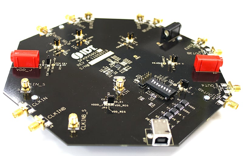
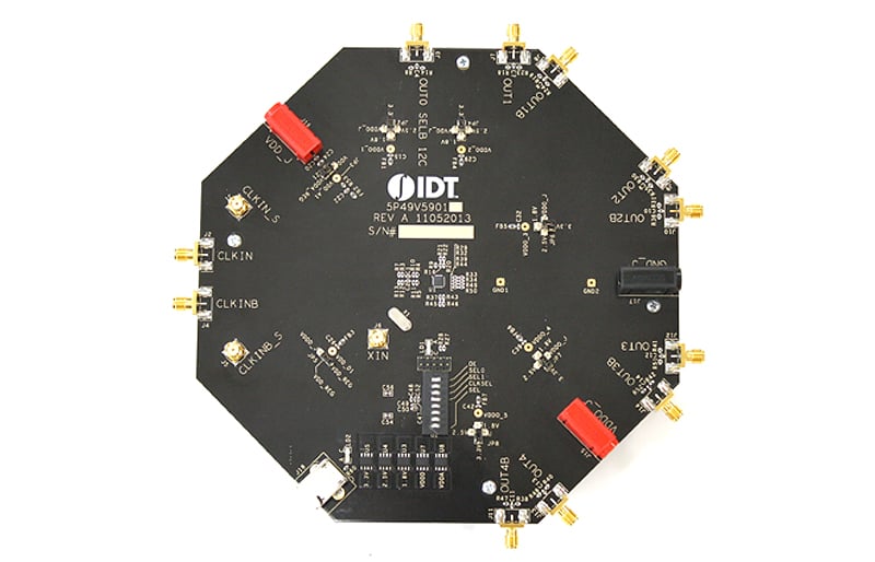
Renesas 5P1103 Programmable buffer outputs can be individually programmed as LVDS, LVPECL, HCSL or two LVCMOS outputs per output pair, with a crystal, LVCMOS, or differential input. There are up to two universal output pairs, as well as a LVCMOS output clock. Output frequencies range from 1 MHz to 200 MHz for LVCMOS and 1 MHz to 350 MHz for differential outputs. Output voltage can be individually selected (1.8 V, 2.5 V or 3.3 V) for each output pair. 5P1103 has two universal outputs and a LVCMOS output. The evaluation board is designed to help the evaluate the 5P1103, the latest addition to the family of programmable devices in Renesas's Timing portfolio.
特性
- 4 Differential Outputs capable of generating any output frequency using Renesas Timing Commander™ software
- SMA connectors for outputs
- When the board is connected to a PC running Renesas Timing Commander Software through USB, the device can be individually programmed as LVDS, LVPECL, HCSL or two LVCMOS outputs per output pair
- 5P1103 has two universal outputs and a LVCMOS output.
应用
Processing table

Tips for Using This Parametric Table:
- Hide Filters button in header: Collapse or expands filters
- Column sort buttons in header: Sort Column alphabetically / numerically descending or ascending
- Reset button in header: Reset all filters to the page default
- Full Screen button in header: Expand the table to full screen view (user must close out of full screen before they can interact with rest of page)
- Export button in header: Export the filtered results of the table to an Excel document
- Filter parts search bar in header: Type to filter table results by part number
- Hide column button in column headers: Select to hide columns in table
- AND / OR toggle switches in header: Toggles the logic of this particular filter to be “AND” or “OR” logic for filtering results
- Multiselect checkboxes at beginning of each row in table: Select these checkboxes to compare products against each other
- Document icon next to product name in row: View the featured document for this product
- Chip icon next to the right of the document icon in row: View the block diagram for this product
- Cart icon to the right of the chip icon: Indicates that samples are available for this product
